
Analog Circuit
Index 16
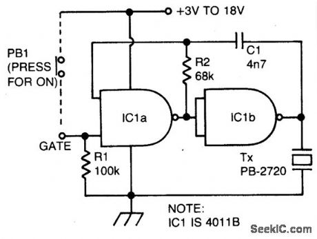
GATED_2_kHz_BUZZER
Published:2009/6/22 23:56:00 Author:May
View full Circuit Diagram | Comments | Reading(685)
SIMPLE_INTERCOM_FOR_NOISY_ENVIRONMENTS
Published:2009/6/22 23:51:00 Author:May
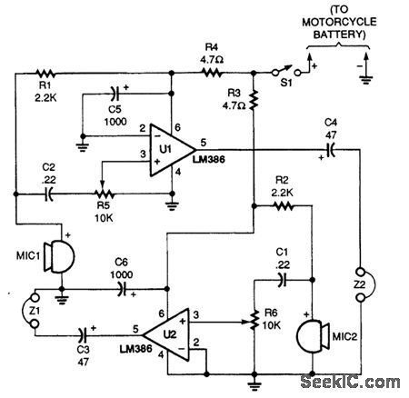
This intercom was originally designed for motorcycle to passenger communications A simple"passenger-to-pilot”ttercom circuit is shown. Two LM386 ICs are connected in a low-gam amplifiercircuit with the headphone output of one paired to the microphone input of the other The microphones are electret elements and the earphones can be of the in-ear type or of the small stereo/monotype that with fit inside a helmet Both amplifiers in the circuit operate at a minimum gain of 20 dB. (View)
View full Circuit Diagram | Comments | Reading(0)
225_W_15_V_OUTPUT_CONVERTER_20_kHz_inverter
Published:2009/6/22 23:47:00 Author:May
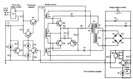
A converter designed to supply t15 Vdc is shown. This converter is several times lighter in weight than an equivalent.
C1 -2500 μF,350 V Electrolyic Q1,Q5,Q6,-2N6307C2—0.1μF Disc Ceramic Q2,Q4 - 2N5052C3—0.1μF Paper Q3—2N5345C4—10 μF Electrolylc Q7-2N4870C5—0.25μF Paper Q8 -2N3905D1—MDA-980-4 Bridge Rectifier Assembly Q9—2N3903 D2,D3,D4,D5-1N5826,20V 15A
All Resistors in Ohms and 1/2 W Unless Otherwise Noted
R1—1,10 W R10-1KR2-100 R11-10KR3-82R12-270R4- 22K R13-1KR5-1.5K,15W R14-7.5KR6-200 R15-2.5KR7-15 R16-5KR8—4.7K 17-3.5KP9-51
T1 - Core -Magnetics Inc 80623-1/2 D-080N1,N2-20 Turns Each,No 30 AWG(Bifilar)N3,N4- 3 Turns Each,No 20 AWG
T2—Core—Arnold 6T 5800 D1N1,N2-100 Turns Each,No. 20 AWG(Bifilar)N3-7 Turns No. 20 AWGN4-12 Turns Each No 12 AWG(No 16 AWG,3 In Parallel)
Z1 —1N4733,5.1 VZ2,Z3 -1N4760,68VZ4- 1N4736 (View)
View full Circuit Diagram | Comments | Reading(983)
PSEUDOGROUND
Published:2009/6/22 23:37:00 Author:May
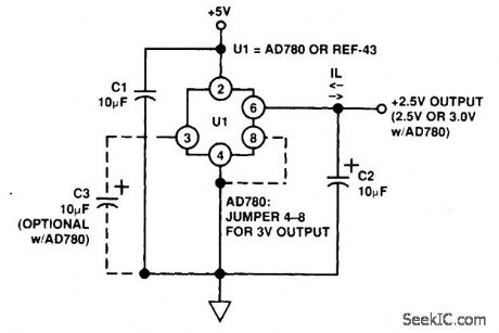
For op-amp circuits, a pseudo ground is often needed; a voltage reference IC can be used. The Analog Devices AD780 is used here for this application. This can sink or source current. (View)
View full Circuit Diagram | Comments | Reading(0)
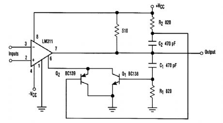
SHORT_CIRCUIT_BEEPER
Published:2009/6/22 23:33:00 Author:May
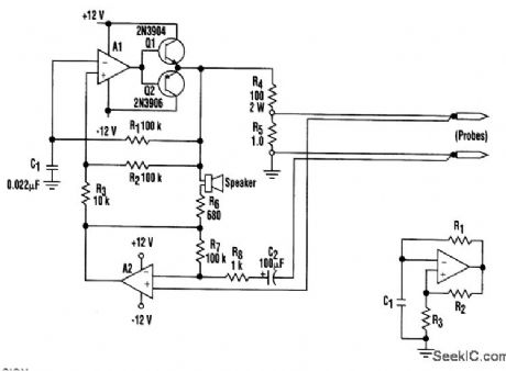
This design offers a way to trace resistance in the milliohm range, right to a short between bridged traces beneath a solder mask. It simply translates resistance into an audible tone, which in-creases in pitch as the measured value approaches zero.In the classic op-amp multivibrator (shown in the inset), oscillation frequency is determined not only by the R1/C1 time constant, but also by the hysteresis set by the R2/R3 resistance ratio. Al in the main figure, with current boosters Q1 and Q2, is this same configuration.Assuming a virtual ground at the output of A2, free-run frequency is about 1 kHz-quite audible through a tiny 8-Ω speaker. Q1 and Q2 deliver a ±10-V squarewave to R4, dumping a ±100 mA through a short circuit placed across the probe tips. R5 ensures that open circuit voltage never ex-ceeds ±0.1 V.AZ monitors the voltage between the probes. The differential input must have its own separate path to the probe tips to eliminate test lead resistance from the measurement. Miniature zip-cord sold as loudspeaker wire makes a tidy two-conductor test lead.When the probes are open, A2's gain equals the R4/R5 divider loss, and the output of both am-plifiers is identical. This has two effects: first, hysteresis is greatly increased and the frequency falls to a low growl; second, the loudspeaker that bridges the two in-phase outputs is effectively silenced.The dead short across the probe tips will return nothing to AZ and the circuit will squeal at its nominal 1-kHz rate. Anything less than a perfect short produces some output from A2, increasing multivibrator hysteresis and lowering the pitch. The circuit has so much 'leverage, and the ear is so sensitive to pitch changes in this range, that it's easy to resolve minute resistance differences.Any general-purpose op amp will suffice in this circuit-a couple of 741s or an equivalent dual. (View)
View full Circuit Diagram | Comments | Reading(962)
VOCAL_STRIPPER
Published:2009/6/22 23:29:00 Author:May
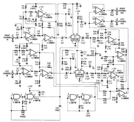
The schematic of the lead vocal filter is shown in the figure. The left and right channel signals are coupled through C1 and'C2 to buffer amps IC4-a and IC4-b. From the buffer amps, the left and right channel signals pass through active crossovers IC5-a and IC5-b, sending all low frequencies to a final mixer IC6-c, and all middle and high frequencies to analog delay lines IC1 and IC2, RD5106256-sam-ple bucket-brigades. Integrated circuit IC2 delays the left-channel signal by 2.4 ms, set by the fixed-frequency clock generated by 1/2IC3, R47, and C24. The right channel signal is delayed by IC1 with a variable-frequency clock generated by 1/2IC3, R48, R49, and C23. Potentiometer R49 is used for phase adjustment.The output of each delay line from IC1 and IC2 passes through low-pass filters IC6-a and -d, and their associated parts, to filter out high-frequency sample-steps produced by IC1 and IC2. Balance control R36 is adjusted for equal amplitude of the left and right channels. ICG-b is a difference am-plifier that cancels all lead vocals that are common to both channels. The resulting signal from ICG-b is remixed with low frequencies by ICG-c and is then sbnt to the output via buffers IC4-c and IC4-d. (View)
View full Circuit Diagram | Comments | Reading(0)
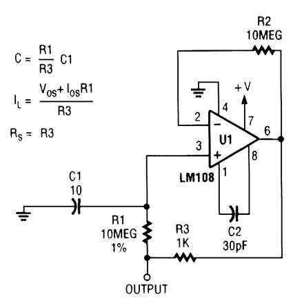
PRACTICAL_DIFFERENTIATOR
Published:2009/6/22 23:18:00 Author:May
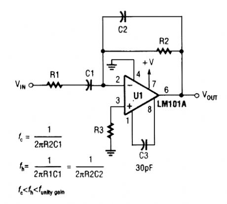
A differentiator has a high-pass charactenstic. Components are chosen by using the design equations. (View)
View full Circuit Diagram | Comments | Reading(0)
CAPACITANCE_MULTIPLIER
Published:2009/6/22 23:17:00 Author:May
View full Circuit Diagram | Comments | Reading(0)
PHASE_LOCKED_LOOP
Published:2009/6/22 23:15:00 Author:May
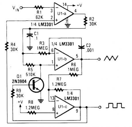
The PLL will lock onto an input signal. Both triangle- and square-wave outputs are available.A quad op amp can be used in this circuit, which should be useful in the audio and LF radio region. (View)
View full Circuit Diagram | Comments | Reading(0)
7805_TURN_ON_CIRCUIT
Published:2009/6/22 23:03:00 Author:May
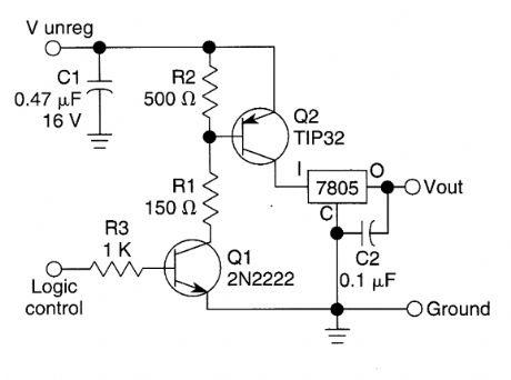
A logic level can control a 7805 regulator with this circuit. Q2 is a series switching transistor controlled by Q1. Q1 is tumed on by a logic voltage to its base. (View)
View full Circuit Diagram | Comments | Reading(2629)
KEY_WIRELESS_RTS_WITH_DATA
Published:2009/6/22 23:02:00 Author:May
This simple keyer supplies both the RTS control and data delay needed to interface a digital ra-dio with an RS-232, data-only system. It supports speeds to 19.2 kbits/s sync or async. (View)
View full Circuit Diagram | Comments | Reading(0)
VIDEO,POWER,AND_CHANNEL_SELECT_SIGNAL_CARRIER
Published:2009/6/22 23:01:00 Author:May

In the video system of Figs. A and B, a single coaxial cable carries power to the remote location, selects one of eight video channels, and returns the selected signal. The system can choose one of several remote surveillance-camera signals, for example, and display the picture on a monitor near the interface box.
The heart of the multiplexer box (A) is a combination 8-channel rnultiplexer and amplifier (ICl). C11 couples the multiplexer's baseband video output to the coax, and L1 decouples the video from dc power arriving on the same line. This power-approximately 30 mA at 10 V-supplies all circuitry in the multiplexer box.
In interface box (B), a desired channel is encoded by three bits, set either by switches as shown or by an applied digital input. Momentary depression of the send button triggers clownconverter IC1 and gated oscillator IC2A to initiate a channel-selection burst. (View)
View full Circuit Diagram | Comments | Reading(0)
MOSFET_DRIVE_CURRENT_BOOSTER
Published:2009/6/22 23:01:00 Author:May
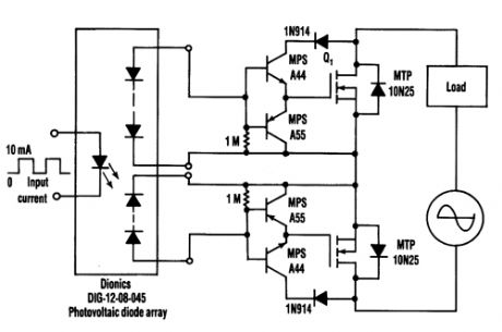

A clean and inexpensive way to eliminate the floating-gate supply is to use the voltage available at the MOSFET's drain to drive its gate. Tying the collector of Q1(a high-voltage, small-signal, 400-V NPN)to the MOSFET's drain supplies sufficient gate-drive voltage when it's needed most-when the MOSFET's drain-to-source voltage is high. Two such circuits used back-to-back form an ac relay.Using the emitter follower attached to the drain increases gate-drive current and decreases the MOSFET's turn-on time by a factor equal to the high-voltage NPN's beta. The resulting drain-to-source voltage fall times depend on the MOSFET's size and its required gate charge. The circuit that's used gives a fall time of 200 ps for an MTP10N2f5 10-A, 250-V MOSFET. With such fall times cutting switching losses, pulse-width modulation at frequencies under 100 Hz is possible.During tune-on, VDS falls rapidly until it reaches the sum of the 1N914 diode's 0.7-V drop, the collector-emitter saturation voltage of Q1, and the gate-to-source voltage required to support the load cur-rent. At that point, the diode array completes the MOSFET's turn-on, unaided by the buffer. This slows the fall of 7,s considerably when it reaches about 5 to 7 V. In high-voltage, low-frequency systems, tail-'ma of VDS is tolerable because the tail's voltage magnitude constitutes a small fraction of the switching voltage. The IN914 makes it possible for VGS to exceed VDS as the MOSFET completes turn-on. (View)
View full Circuit Diagram | Comments | Reading(0)
PHOTODIODE_LOG_CONVERTER_TRA_NSMITTER
Published:2009/6/22 23:00:00 Author:May
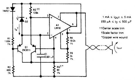
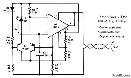
A logarithmic conversion is made on the output current of a photodiode to compress a fourdecade, light-intensity variation into a standard transmission range. The circuit is balanced at midrange, where R3 should be chosen so that the current through it equals the photodiode current. The log-conversion slope is temperature compensated with R6. Setting the reference output to 1.22 V gives a current through R2 that is proportional to absolute temperature because of D1 so that this level-shift voltage matches the temperature coefficient of R6. C1 has been added so that large-area photodiodes with high capacitance do not cause frequency instabilities. (View)
View full Circuit Diagram | Comments | Reading(0)
TELEPHONE_HOLD_CIRCUIT
Published:2009/6/22 22:57:00 Author:May
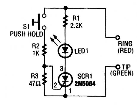
When S1 is pressed, the SCR fires, and places LED1 and R1 across the phone line. The line volt-age drops to about 20 V, which holds the connec-tion to the phone company's central office. (View)
View full Circuit Diagram | Comments | Reading(0)
SET_TIME_WINDOWS_WITHIN_A_CLOCK
Published:2009/6/22 22:49:00 Author:May
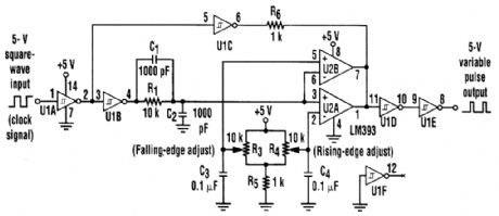
At times, it is necessary to produce pulses of adjustable width and whose start times might vaty with reference to a master clock. The input signal is inverted and buffered by U1A, while U1B and U1C reinvert the signal to produce square, buffered renditions of the input signal. Potentiometers R3 and R4 set references for the comparators.The input polarity of U2A keeps its output transistor tumed on until the voltage at the nonin-verting input exceeds the reference set by R4 (the rising edge adjustment). When this reference voltage is exceeded, the output transistor is turned off and the output signal is pulled up via R6.Meanwhile, the input polarity of U2B keeps its output transistor turned off until the voltage at the in-verting input exceeds the reference set by R3 (the falling edge adjustment). When this reference voltage is surpassed, the output transistor of U2B is turned on, pulling the output signal low through the wired-OR conftguration of U2. The output of U2 is then double-inverted and buffered by U1D and U1E. What results is a pulse whose start time (rising edge) can be adjusted by R4, and whose stop time (falling edge) can be adjusted by R3.The output of the comparators is pulled up to the input waveform through resistor R6 to U1C.This prevents the comparators from switching during the low cycle of the input waveform, regard-less of the positions of R3 and R4. This has the effect of locking out changes during the low period of the input signal, and would probably require additional logic if it were done strictly in the digital domain.The circuit, with the component values shown, works well between about 50 and 150 kHz. (View)
View full Circuit Diagram | Comments | Reading(0)
PROGRAMMABLE_CAPCITOR_CIRCUIT
Published:2009/6/22 22:42:00 Author:May
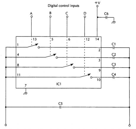
IC1 CD4066 quad bilateral switchG1 10-μF, 25-V capacitorC2 22-μF, 25-V capacitorC3 47-μF, 25-V capacitor04 100-μF,25-V capacitorC5 1-μF, 25-V capacitor06 0.1-μF, 25-V capacitorThe programmable capacitor can be very useful in circuits where you need to switch capacitance values. Remember that the ON resistance of IC1 appears in series with the capacitors and must be taken into account in some applications as it is not negligible.
(View)
View full Circuit Diagram | Comments | Reading(729)
SUPPRESS_JITTER_WITH_HYSTERESIS
Published:2009/6/22 22:40:00 Author:May
When the comparator's output changes its state from low to high, the rising edge of the output pulse, differentiated by the C1/R1 chain, opens Q1. This blocks comparator M via its strobing input and sustains its output in the H state for a period of time, defined by the time constant R,Ct After C1 is charged by the current flowing through R1, Q1 is shut off and the comparator is released. When the comparator's output state changes from high to low, a similar process, involving elements R2, C2, and Q2, occurs. In many applications, the output transition in only one direction is of vital importance, and the elements, which provide temporal hysteresis for the opposite direction transition, can be omitted. (View)
View full Circuit Diagram | Comments | Reading(726)
10_MHz_FREQUENCY_STANDARD
Published:2009/6/22 22:39:00 Author:May
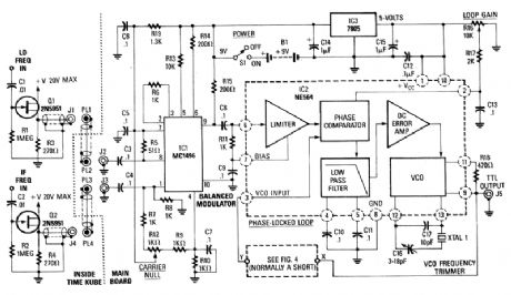
A Radio Shack 10-MHz receiver is used as a basis for this circuit. The L.O. and IF frequencies are added. When the receiver is tuned to 10 MHz(WWV), the sum of the L.O. and IF are used to phase lock a VCO to the 10-MHz signal. By using a divider in the Ioop, 2.5 or 5 MHz can be used as well. (View)
View full Circuit Diagram | Comments | Reading(1097)
TELEPHONE_VOICE_MAIL_ALERT
Published:2009/6/22 22:36:00 Author:May
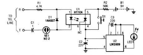
The circuit is built around a couple of low-cost ICs: an H11C4 optoisolator/coupler with an SCR output (U1) and an LM3909 LED flasher (U2). It is connected to the phone line in the same manner as any extension phone. A ring signal on the telephone activates the optoisolator/SCR, and causes U2 to flash LED1. This flash signifies that a ring signal has been received. (View)
View full Circuit Diagram | Comments | Reading(1809)
| Pages:16/24 1234567891011121314151617181920Under 20 |
Circuit Categories
power supply circuit
Amplifier Circuit
Basic Circuit
LED and Light Circuit
Sensor Circuit
Signal Processing
Electrical Equipment Circuit
Control Circuit
Remote Control Circuit
A/D-D/A Converter Circuit
Audio Circuit
Measuring and Test Circuit
Communication Circuit
Computer-Related Circuit
555 Circuit
Automotive Circuit
Repairing Circuit