
Analog Circuit
Index 3
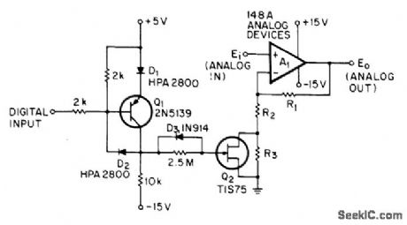
SINGLE_TONE_SIGNALING
Published:2009/7/14 21:11:00 Author:May
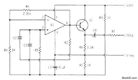
Wien-bridge oscillator using 741 opamp drives 2N2924 or equivalent NPN transistor to generate stable audio tone for signaling over telephone lines Tuning capacitor(C2 and C3 are equal)and resistor(R2 and R3 are equal) values range from 0.1μF and 15.9K for 100 Hz to 0.005 μF and 6.3K for 5000Hz For other frequencies use f =0.159/R2C2 With 12-V supply tone output is about 7 V P-P Select R7 to match impedance of driven circuit.-C. D Rakes. Integrated Circuit Projects. Howard W Sams . Indianapolis IN 1975.p 55-60. (View)
View full Circuit Diagram | Comments | Reading(1424)
SIMPLE_VCO_DRIVER
Published:2009/7/14 20:43:00 Author:May
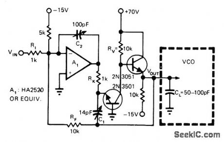
Provides full output of 60 V P-P up to 1 MHz Slew rate is 200 V/μs, and small-signal bandwidth is 5 MHz. Uses fastinput opamp, voltage buffer, and simple compensation technique. C2 is trimmed for stability, while C1 is adjusted to increase slew rate and bandwidth. -H Bunin, Low Cost VCO Driver Amplifiers Really Perform If Designed Right, EDN Magazine, Oct 5. 1974, p 51-55. (View)
View full Circuit Diagram | Comments | Reading(1185)
IMPEDANCE_CONVERTER
Published:2009/7/14 7:18:00 Author:May
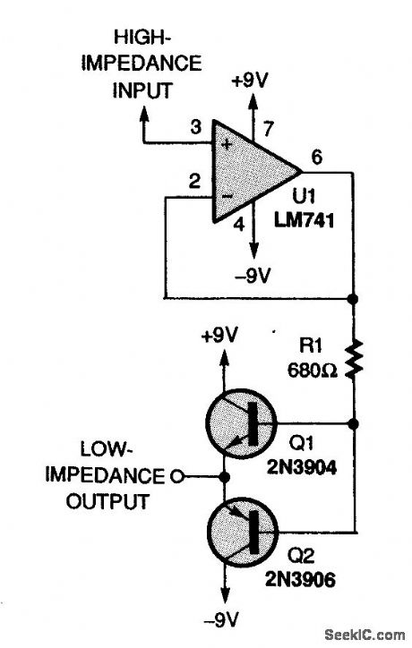
This circuit is a high-input-impedance-to-low-output-impedance converter circuit with unity voltage gain. In the circuit, an LM741 op amp, U1, is connected in a voltage-follower circuit that drives a complementary transistor-emitter-follower circuit. The output of the circuit can be used to drive low-current lamps, relays, speakers, etc. The feedback can be taken from the output to pin 2 of the LM741 if it is desired to include Q1and Q2 in the feedback loop. (View)
View full Circuit Diagram | Comments | Reading(0)
PROGRAMMABLE_0_825_Hz_PULSES
Published:2009/7/14 5:13:00 Author:May
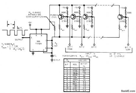
Inexpensive pulse generator is programmable in 0.4-Hz steps from 0 to 825 Hz, and can be modified to extend range to 200 kHz, Circuit uses 555 connected in astable mode, with timing resistor RA replaced by 11 sets of timing resistors and switching transistors. Inputs and outputs are TTL-compatible. When bit input is high (0), its associated transistor is turned off. When bit input is low (1), transistor is on, allowing C1 to charge. When more than one input is low, charging is through parallel combination of resistors. Width of output pulse T1 is constant over frequency range.-E. G. Laughlin, Inexpensive Pulse Generator Is Logic Programmable, EDN Magazine, Aug. 20, 1974, p 92. (View)
View full Circuit Diagram | Comments | Reading(1133)
GAIN_PROGRAMMABLE
Published:2009/7/14 4:41:00 Author:May
Gain of non-inverting opamp can be programmed with standard digital logic levels. With input at 0 V, Q1 is turned on but is held out of saturation by Schottky diode D2. Resulting opamp gain is (R1 + R2)/R2.If R2 is 1.13 kilohms and R1 10 kilohms, gain is 10. When input is 5 V, Q1 is off and gate of Q2 is driven to -15 V. Gain now becomes (R1 + R2 + R3)/(R2 + R3). If R3 is 8.87 kilohms, gain is 2.-K. Karash, Gain-Programmable Amplifier, EEE Magazine, Sept. 1970, p 89. (View)
View full Circuit Diagram | Comments | Reading(1090)
ANALOG_SAMPLE_HOLD_CIRCUIT
Published:2009/7/14 3:25:00 Author:May
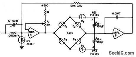
Uses diode bridge as switching circuit. Operational amplifier A delivers maximum current of 10 ma. Chopper-stabilized operational amplifier B delivers 100 v at 10 ma.-T. A. Brubaker, Precision Analog Memory Has Extended Frequency Response, Electronics, 34:39,p 141-143. (View)
View full Circuit Diagram | Comments | Reading(832)
TEMPERATURE_COMPENSATED_DECODER
Published:2009/7/14 3:24:00 Author:May
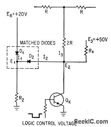
Matched diodes in ladder-type network decoder change one reference voltage of transistor switch to compensate for temperature effects-C. R. Pearman and A. E. Popodi, How to Design High-Speed D-A Converters,Electronics,37:8,p 28-32. (View)
View full Circuit Diagram | Comments | Reading(717)
PULSE_WIDTH_TO_ANALOG_DEMODULATOR
Published:2009/7/14 3:23:00 Author:May
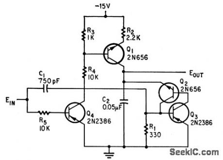
Circuit integrates incoming pulse and holds final value until next pulse arrives, Output then returns to zero for next integration. Output range is 0 to 10 v for input pulse width range of 0 to 1 microsec.-D. Knowlton, Modulated Pulse Width Converted to Analog Voltage, Electronics, 38:20, p 99-100. (View)
View full Circuit Diagram | Comments | Reading(958)
POTENTIOMETER_ERROR_COMPUTER
Published:2009/7/14 3:17:00 Author:May
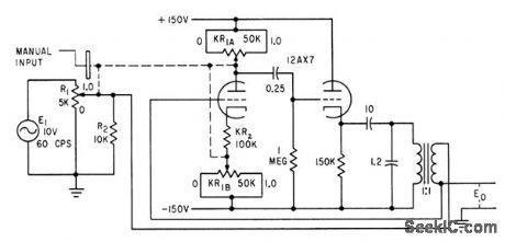
Compensation technique eliminates need for precise high-gain isolation amplifiers when linear potentiometers are used as precision voltage dividers in analog computing circuits. Error is reduced by factor of 100.-M. Kanner, How to Reduce Errors in Loaded Potentiometers, Electronics, 32:34, p 34-35. (View)
View full Circuit Diagram | Comments | Reading(805)
ENCODER
Published:2009/7/14 3:09:00 Author:May
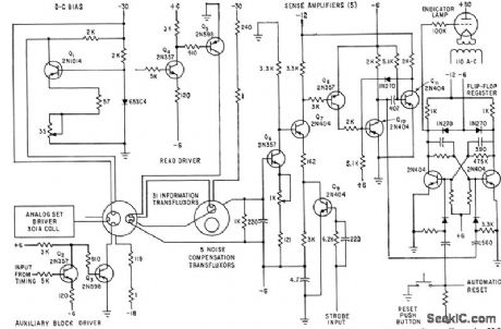
Used between fransfluxor and digital shift register of converter that changes analog inputs to six-bit binary Gray code.-N. Aron and C. Granger, Analog-To-Digital Converter Uses Transfluxors,Electronics,35:20,p 62-66. (View)
View full Circuit Diagram | Comments | Reading(954)
POLARITY_DETECTOR
Published:2009/7/14 3:07:00 Author:May
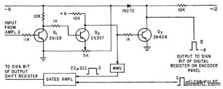
Q1-Q2 amplify negative analog samples greater than 100 mv, to provide sharp pulse output for driving monostable mvbr in analog-digital converter.-N, Aron and C, Granger, Analog-To-Digital Converter Uses Transfluxors Electronics, 35:20, p 62-66. (View)
View full Circuit Diagram | Comments | Reading(1052)
FET_VOLTAGE_COMPARAIOR
Published:2009/7/14 3:03:00 Author:May
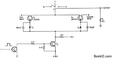
Circuit uses spdt configuration. Used to switch reference voltage (such as ground) to successive points on binary voltage ladder until comparator determines that output of ladder is equal to that of unknown voltage. Sine and square wave inputs at A and B produce output at C. Used also for low-level differential switching.-J. Gulbenk and T. F. Prosser, How Modules Make Complex Design Simple, Electronics, 37:32, p 50-54. (View)
View full Circuit Diagram | Comments | Reading(715)
TUNNEL_DIODES_READ_5_APERTURE_CORE
Published:2009/7/14 3:02:00 Author:May
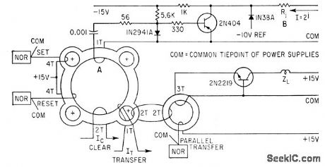
Circuit also controls switching of binary weighted current generators used in analog-digital converter. W. G. Trabold, Tunnel Diodes Save Parls-Continuous Readout of Magnetic Cores, Electronics, 36:36, p 38-39. (View)
View full Circuit Diagram | Comments | Reading(749)
WEIGHTING_CIRCUIT
Published:2009/7/14 3:00:00 Author:May
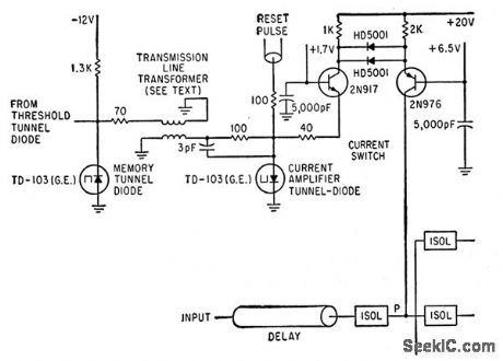
Circuit introduces precise amount of current into point P within few nsec in response to output of threshold tunnel diode, contributing to accurate conversion of wideband analog signals into 64 levels that are described by six bits of binary language.-H. R. Schindler, Semiconductor Circuits in a UHF Digital Converter, Electronics, 36;35, p 37-40. (View)
View full Circuit Diagram | Comments | Reading(876)
50_MC_SAMPLING_AND_THRESHOLD_CIRCUIT
Published:2009/7/14 2:58:00 Author:May
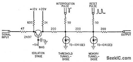
Threshold tunnel diode receives signal current to be sampled and interrogation pulses repeating at 50 Mc. Diode fires when signal current is below threshold level, making memory tunnel diode switch into its high-voltage state. Current level differences of less than 50 microamp can be resolved in 0.3 nsec, sufficient for converting input into six bits corresponding to 64 levels.-H. R. Schindler, Semiconductor Circuits in a UHF Digital Converter, Electronics, 36:35, p 37-40.
(View)
View full Circuit Diagram | Comments | Reading(871)
12_V_STROBOSCOPE
Published:2009/7/14 1:37:00 Author:May
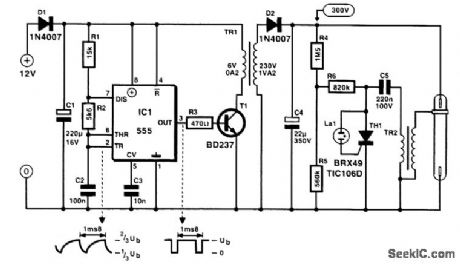
Diode Dl is a polarity-protection device that can be omitted. A 555 is used as an astable with a frequency of about 0.7 kHz. When T1 is on, a current flows through the 6-V winding of TR1. When the collector voltage of T1 is nearly 0, the potential at the anode of D2 must be negative. When T1 becomes reverse-biased, its collector voltage rises to about 12 V and the potential at the anode of D2 must then be positive so that C4 can be charged Never operate the converter without a load. It is, perhaps, advisable to shunt C4 with a 100-kΩ, 1-W resistor. The converter charges C4 to about 300 V. This causes a potential at junction R6-05 of about 100 V. The neon lamp then comes on, so a gate current flows into the thyristor. This comes on and clears the way for C5 to discharge through TR2.This starting transformer produces a secondary voltage of a few thousand volts. This is sufficient for the xenon tube to strike and at the same time discharge C4. Then the operation can start again. The circuit draws a current of about 250 mA, but this depends on the flashing rate and the type of xenon tube. (View)
View full Circuit Diagram | Comments | Reading(1204)
600_W_TRIGGERED_SCR
Published:2009/7/13 22:15:00 Author:May
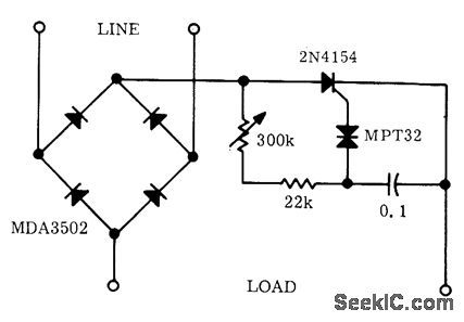
2N4154 SCR is operated from DC output of bridge rectifier and triggered by MPT32 at setting determined by position of 300K pot. Circuit provides full-wave DC control of lamp and other loads up to 600 W, using relaxation oscillator operating from DC source.- SCR Power Control Fundamentals, Motorola, Phoenix, AZ, 1971, AN-240, p 6. (View)
View full Circuit Diagram | Comments | Reading(1123)
NEON_INDICATOR_SCALER
Published:2009/7/13 21:10:00 Author:May
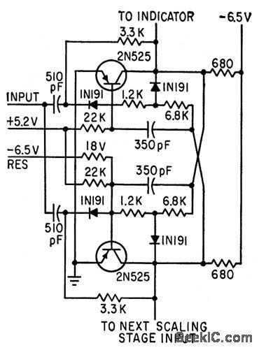


Battery-powered stage uses binary scaling circuit with nonsaturated temperature-compensated transistors, as elements of scale-of-64 circuit driving 4-dight mechanical register.-F.E. Armstrong. Battery Powered Portable Scaler.Electronics.33:19,p74-75 (View)
View full Circuit Diagram | Comments | Reading(843)
LINEAR_RAMP
Published:2009/7/13 6:04:00 Author:May
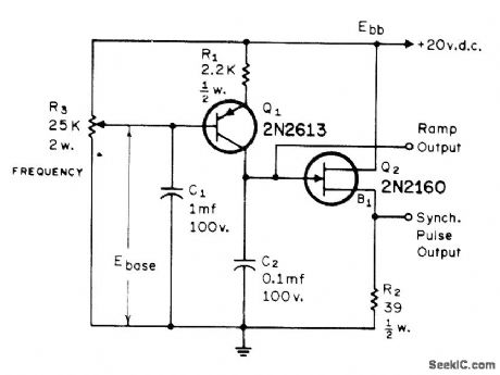
Free-running ramp generator has excellent linearity and repetition rate independent of supply voltage. C2 is charged at constant current through a, and is discharged by Q2. R2 provides sync pulse during retrace. Repetition rate of ramp is controlled by R3, from about 100 to 4000 Hz. Output voltage is 10 V P-P, and sync pulse amplitude is 5 V P-P.-J. J. Nagle, Voltage Independent Ramp Generator, CQ, Sept. 1972, p 61 and 98. (View)
View full Circuit Diagram | Comments | Reading(0)
HALF_WAVE_SYNCHRONOUS_RECTIFLER
Published:2009/7/12 23:51:00 Author:May
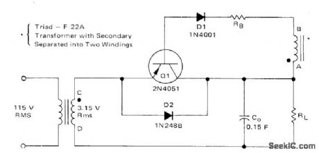
Transistoral is synchronously biased on by AC input voltage to give efficient low-voltage regulation. When points A and C are positive with respect to points B and D, base-emitter junction of Q1 is forward-biased and collector current flows through load RL. On negative alternations,Q1 is reverse-biased and transistor is blocked.-B. C. Shiner, Improving the Efficiency of Low Voltage, High-Current Rectification, Motorola, Phoenix, AZ, 1973, AN-517, p 3. (View)
View full Circuit Diagram | Comments | Reading(945)
| Pages:3/24 1234567891011121314151617181920Under 20 |
Circuit Categories
power supply circuit
Amplifier Circuit
Basic Circuit
LED and Light Circuit
Sensor Circuit
Signal Processing
Electrical Equipment Circuit
Control Circuit
Remote Control Circuit
A/D-D/A Converter Circuit
Audio Circuit
Measuring and Test Circuit
Communication Circuit
Computer-Related Circuit
555 Circuit
Automotive Circuit
Repairing Circuit