
Analog Circuit
Index 5
ERROR_TAKEOFF_REDUCES_DISTORTION
Published:2009/6/29 1:52:00 Author:May
Nonlinear distortion is reduced in singleended amplifier by producing voltage proportional to distortion and amplifying this error voltage in such a way thatit can be used to reduce distortion at output. Circuit uses 741 opamps and MJ4000 power Darlington transistors. Technique overcomes basic Iimitation of negative feedback wherein feedback loop gain decreases as frequency increases. Artide also gives variation of circuit more suitable for power amplifier, and describes circuit operation in detail.-A. M. Sandman, Reducing Amplifier Distortion, Wireless World, Oct. n974, p 367-371. (View)
View full Circuit Diagram | Comments | Reading(766)
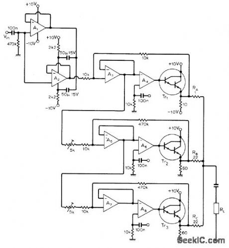
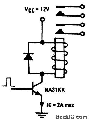
DRIECT_DC_DRIVE_INTERFACE_OF_A_TRAC
Published:2009/6/29 1:42:00 Author:May
View full Circuit Diagram | Comments | Reading(988)
50_kHz_BANDWIDTH
Published:2009/6/29 1:41:00 Author:May
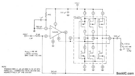
Three transistor pairs in CA3600E array are parallel-connected with output stage of CA3130 bipolar M0S opamp to boost current-handling capability about 2.5 times. Use of feedback gives closed-loop gain of 48 dB. Typical large-signal bandwidth is 50kHz for 3 dB down-″Circuit ldeas for RCA Linear ICs、″RCA Solid State Division、Somerville,NJ,1977,p 12 (View)
View full Circuit Diagram | Comments | Reading(755)
HIGH_SPEED_SHIELD_LINE_DRIVER_
Published:2009/6/29 1:39:00 Author:May
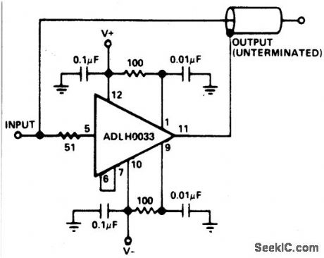
View full Circuit Diagram | Comments | Reading(679)
COAXIAL_CABLE_DRIVER_
Published:2009/6/29 1:38:00 Author:May
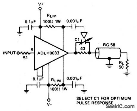
View full Circuit Diagram | Comments | Reading(759)
VARIABLE_BIPOLAR_CLAMPING
Published:2009/6/29 1:37:00 Author:May
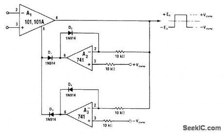
Precision comparator provides independent regulation of both output voltage limits without connection to comparison inputs. A2 and A3 are complementary precision rectifiers having independent positive and negative reference voltages, with both rectifiers operating in dosed loop through A1. A2 senses positive peak of Eo and maintains it equal to +Vclamp by adjusting voltage applied to D1. A3 and D3 perform similar function on negative peaks. Feedback network around output stage of A1 regulatesoutput voltage independently of inputs to A1. —W. G. Jung, IC Op-Amp Cookbook, Howard W. Sams, Indianapolis, IN, 1974, p 228-229. (View)
View full Circuit Diagram | Comments | Reading(936)
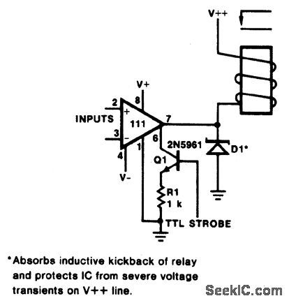
SOLENOID_DRIVER_
Published:2009/6/29 Author:May
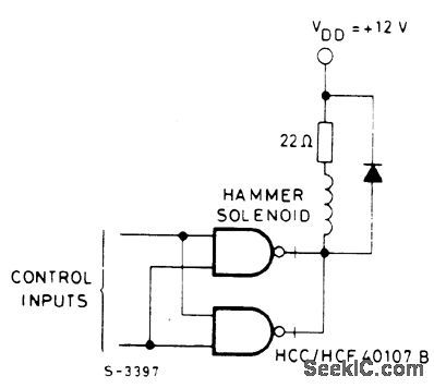
View full Circuit Diagram | Comments | Reading(916)
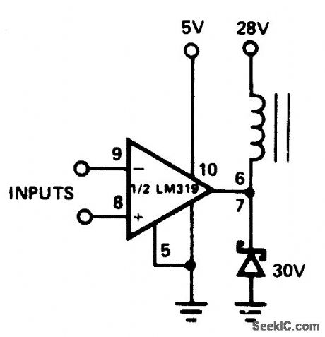
CRT_YOKE_DRIVER_
Published:2009/6/28 23:59:00 Author:May
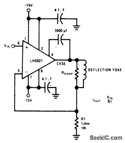

Circuit Notes A 500 mV peak-to-peak triangular waveform about ground is input to the amplifier,gtvmg rlse to a 100 mA peak current to theinductor,. (View)
View full Circuit Diagram | Comments | Reading(1009)
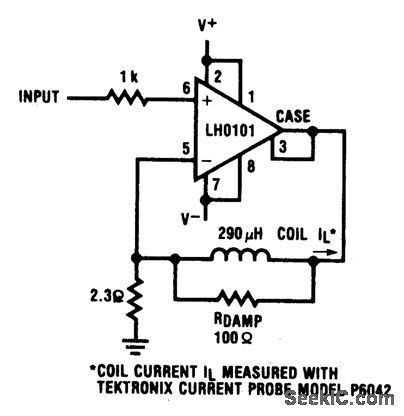
CRT_DEFLECTION_YOKE_DRIVER_
Published:2009/6/28 23:57:00 Author:May

View full Circuit Diagram | Comments | Reading(877)
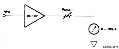
HIGH_IMPEDANCE_METER_DRIVER_
Published:2009/6/28 23:56:00 Author:May
View full Circuit Diagram | Comments | Reading(778)
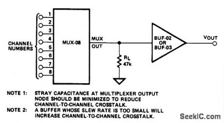
HIGH_SPEED_LINE_DRIVER_FOR_MULTIPLEXERS
Published:2009/6/28 23:49:00 Author:May
View full Circuit Diagram | Comments | Reading(747)
BIFET_CABLE_DRIVER
Published:2009/6/28 23:48:00 Author:May

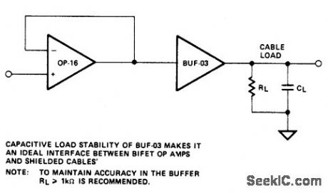
View full Circuit Diagram | Comments | Reading(677)
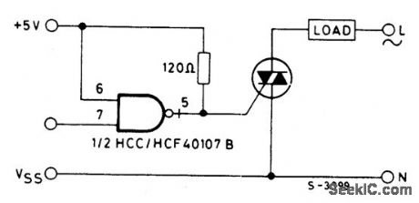
RELAY_DRIVER__
Published:2009/6/28 23:46:00 Author:May
View full Circuit Diagram | Comments | Reading(787)
CAPACITIVE_LOAD_DRIVER
Published:2009/6/28 23:42:00 Author:May
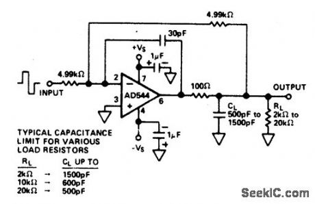
View full Circuit Diagram | Comments | Reading(838)
HIGH_SPEED_LASER_DIODE_DRIVER
Published:2009/6/28 23:41:00 Author:May
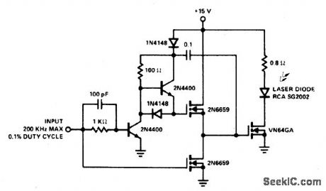
Circuit NotesA faster driver, can supply higher gate current to switch the VN64GA very quickly. The circuit uses a VMOS totemple, stage to drive the high power switch. (View)
View full Circuit Diagram | Comments | Reading(1518)
LOW_EMISSION_CD
Published:2009/6/28 23:38:00 Author:May
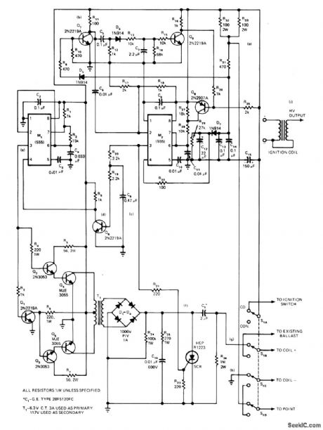


Solid-state capacitor-discharge ignition system improves combustion efficiency by increasing spark duration. For 8-cylinder engine, normal CD system range of 180 to 300,ttS is increased to 600 ps below 4000 rpm the discharge lasts for one cycle or 300 pts because at higher speeds the power cycle has shorter times. Circuit uses 555 timer M1 as 2-kHz oscillator, with Q1-Q3 providing drive to Q4-Q5 and T, for converting battery voltage to about 400 VDC at output of bridge rectifier. When dis-tributor points open,Q7 turns on and triggers M2 connected as mono that provides gate drive pulses for SCR. Article describes operation of circuh in detail and gives waveforms at points a-i.-C. C. Lo, CD lgnition System Produces Low Engine Emissions, EDN Magazine, May 20, 1976, p 94, 96, and 98. (View)
View full Circuit Diagram | Comments | Reading(2144)
LINE_DRIVER
Published:2009/6/28 23:23:00 Author:May
View full Circuit Diagram | Comments | Reading(0)
50_OHM_DRIVER
Published:2009/6/28 23:21:00 Author:May
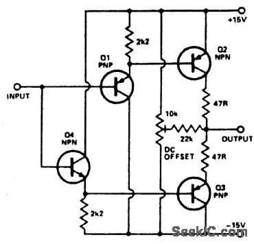
Circuit Notes
To buffer a test generator to the outside world requires an amplifier with sufficient bandwidth and power handling capability. The circuit is a very simple unity gain buffer. It has a fairly high input impedance, a 50 ohm output impedance, a wide bandwidth, and high slew rate. The circuit is simply two pairs of emitter ollowers. The base emitter voltages of Q1 and Q2 cancel out, and so do those of Q3 and Q4.The preset is used to zero out any small dc offsets due to mismatching in the transistors. (View)
View full Circuit Diagram | Comments | Reading(1733)
DRIVER_CIRCUITS
Published:2009/6/28 23:11:00 Author:May
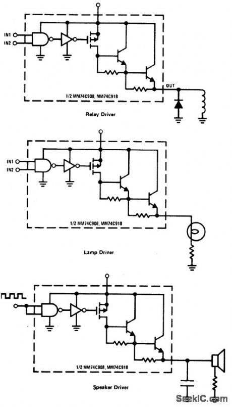
Circuit NotesCM0S drivers for relays, lmps,speakers,etc, offers extremely low standby power. At Vcc = 15V, power dissipation per package is typically 750 nW when the outputs are not drawing current. Thus, the drivers can be sitting out on line (a telephone line, for example) drawing essentially zero current until activated. (View)
View full Circuit Diagram | Comments | Reading(798)
DECADE_FREQUENCY_DIVIDER
Published:2009/6/28 23:05:00 Author:May
View full Circuit Diagram | Comments | Reading(864)
| Pages:5/24 1234567891011121314151617181920Under 20 |
Circuit Categories
power supply circuit
Amplifier Circuit
Basic Circuit
LED and Light Circuit
Sensor Circuit
Signal Processing
Electrical Equipment Circuit
Control Circuit
Remote Control Circuit
A/D-D/A Converter Circuit
Audio Circuit
Measuring and Test Circuit
Communication Circuit
Computer-Related Circuit
555 Circuit
Automotive Circuit
Repairing Circuit