
Analog Circuit
Index 11
SUPERHET_FRONT_END
Published:2009/6/24 4:36:00 Author:May
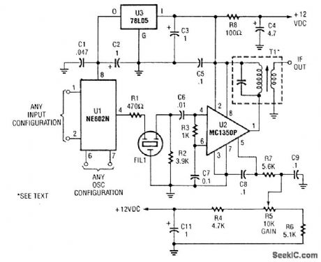
This superhet receiver front end is simple and uses an NE602 followed by an MC1350 IF amplifier. (View)
View full Circuit Diagram | Comments | Reading(0)
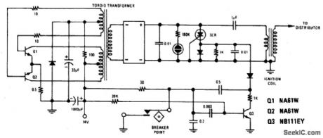
CAPACITOR_DISCHARGE_IGNITION_SYSTEM
Published:2009/6/24 4:22:00 Author:May
View full Circuit Diagram | Comments | Reading(0)
DIFFERENTIAL_THERMOMETER
Published:2009/6/24 4:18:00 Author:May
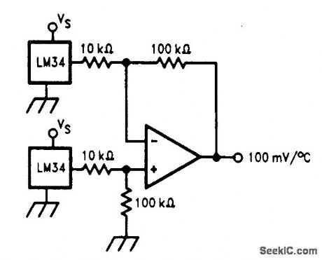
The differential thermometer shown in the figure produces an output voltage which is proportional to the temperature difference between two sensors. This is accomplished by using a dif-ference amplifier to subtract the sensor outputs from one another and then multiplying the differ-ence by a factor of 10 to provide a single-ended output of 100 mV per degree of differential tem-perature. (View)
View full Circuit Diagram | Comments | Reading(0)
UNIVERSAL_WIPER_DELAY
Published:2009/6/24 4:04:00 Author:May
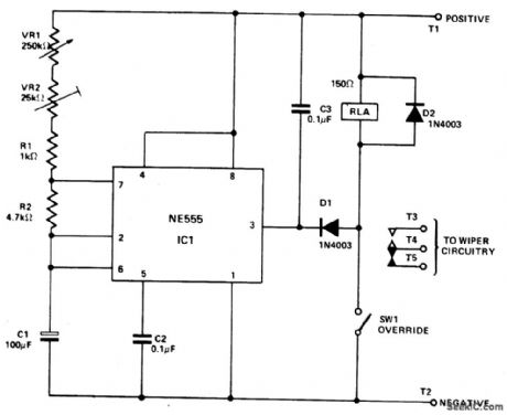
IC1 is connected in the astable mode, driving RLA. C3, Dl, and D2 prevent spikes from the relay coil and the wiper motor from triggering IC1. VR2 is adjusted to give the minimum delay time required. VR1 is the main delay control and provides a range of from about 1 second to 20 seconds. SW1 is an over-ride switch to hold RLA permanently on (for normal wiper operation). The relay should have a resistance of at least 150 ohms and have heavy duty contacts. The suppression circuit may be needed for the protection of IC1. (View)
View full Circuit Diagram | Comments | Reading(0)
VARIABLE_SENSITIVITY_PHOTOTRANSISTOR_CIRCUIT
Published:2009/6/24 4:00:00 Author:May
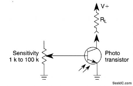
A variable resistor is used to vary the light-level response of a phototransistor. Phototransistors are more light sensitive than photodiodes, but they generally have poorer frequency response. (View)
View full Circuit Diagram | Comments | Reading(3139)
GASOLINE_ENGINE_TACHOMETER
Published:2009/6/24 3:59:00 Author:May
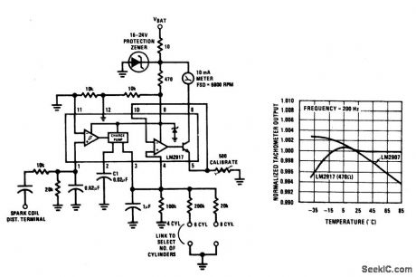
This tachometer can be set up for any number of cylinders by linking the appropriate timing resistor as illustrated. A 500 ohm trim resistor can be used to set up final calibration.A protection circuit composed of a 10 ohm resistor and a zener diode is also shown as a safety precaution against the transients which are to be found in automobiles. (View)
View full Circuit Diagram | Comments | Reading(820)
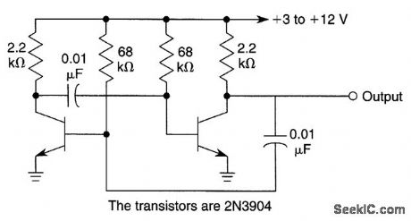
ASTABLE_MULTIVIBRATOR
Published:2009/6/24 3:49:00 Author:May

View full Circuit Diagram | Comments | Reading(0)
ASTABLE_WITH_VARIABLE_PULSE_WIDTH
Published:2009/6/24 3:44:00 Author:May
This produces a positive variable width pulse and has a symmetry control. R1 and R2 control the pulse width and symmetry. (View)
View full Circuit Diagram | Comments | Reading(0)
DISC_TAPE_PHASE_MODULATED_READBACK_SYSTEMS
Published:2009/6/24 3:44:00 Author:May
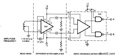
View full Circuit Diagram | Comments | Reading(0)
PHONE_LINE_SIMULATOR
Published:2009/6/24 3:44:00 Author:May
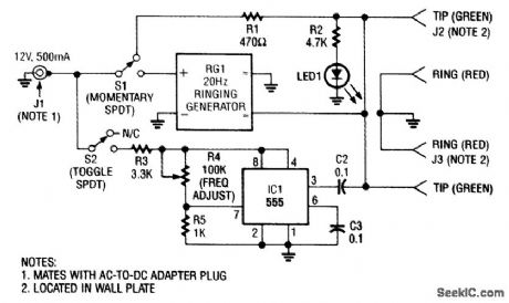
This device contains a ringing generator and a tone oscillator. The tone oscillator is set to either 350 or 440 Hz. The ringing generator is a potted module delivering 86 Vac at 20 Hz. It is available from a source listed in the reference. (View)
View full Circuit Diagram | Comments | Reading(1542)
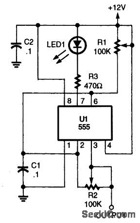
ASTABLE
Published:2009/6/24 3:41:00 Author:May
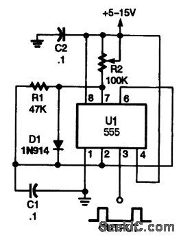
At the instant that power is applied to the 555 astable, timing capacitor C1 is initially discharged, causing the output of the chip output at pin 3 to be high. Once C1 has charged to about 2/3 of the supply voltage, its output goes low, and the discharge transistor turns on, draining the charge on C1. (View)
View full Circuit Diagram | Comments | Reading(0)
TELEPHONE_AUDIO_INTERFACE
Published:2009/6/24 3:39:00 Author:May
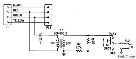
The telephone audio interface-essentially, a simple isolation/couple circuit-isolates the phone line from any connected audio circuit without presenting any danger to the phone line, the equip-rnent, or the user. (View)
View full Circuit Diagram | Comments | Reading(0)
BISTABLE_MULTIVIBRATOR
Published:2009/6/24 3:38:00 Author:May
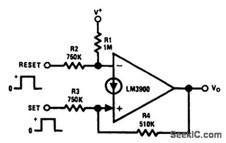
Positive feedback is provided by resistor R4, which causes the latching. A positive pulse at the set input causes the output to go high and a reset positive pulse will return the output to es-sentially 0 Vdc. (View)
View full Circuit Diagram | Comments | Reading(0)
BELL_SYSTEM_202_DATA_ENCODER
Published:2009/6/24 3:38:00 Author:May
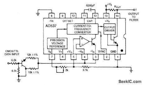
The AD537 is well-suited for frequency-shift modulator and demodulator applications. Requir-ing little power, it is especially appropriate for using phone-line power. The Bell-System 202 data en-coder shown here delivers the mark frequency of 1.2 kHz with the data input low. When the input goes high, the timing current increases to 165 μA and generates the space frequency of 2.2 kHz. The trim shown provides a ±10% range of frequency adjustment. The output goes to the required band-pass filter before transmission over a public telephone line. A complementary demodulator is easy to implement. (View)
View full Circuit Diagram | Comments | Reading(0)
ASTABLE_MULTIVIBRATOR_WITH_STARTING_NETWORK
Published:2009/6/24 3:35:00 Author:May
This circuit will start with a slowly rising supply voltage waveform. (View)
View full Circuit Diagram | Comments | Reading(1291)
TELEPHONE_CALL_RESTRICTOR
Published:2009/6/24 3:34:00 Author:May
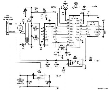
This circuit is designed to restrict phone calls with the area codes: 900, 976, and 540. This device uses a microcontroller to compare the DTMF decoded tones with telephone numbers stored in EEP-ROM (IC3). This device requires a programmed microcontroller. Software and details of program-ming can be found in the original magazine article. (View)
View full Circuit Diagram | Comments | Reading(0)
CALLER_ID_CIRCUIT
Published:2009/6/24 3:33:00 Author:May
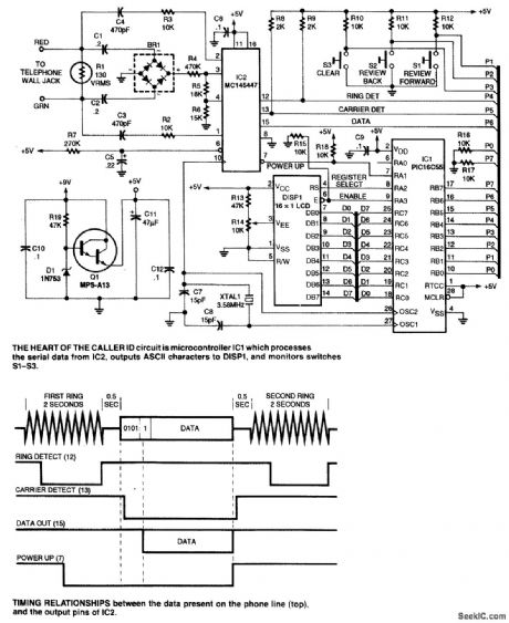
This circuit requires programming of the microcontroller. Software information is available from the reference in the original article. (View)
View full Circuit Diagram | Comments | Reading(0)
PHOTORECEIVER_OPTIMIZED_FOR_NOISE_AND_RESPONSE
Published:2009/6/24 3:28:00 Author:May
View full Circuit Diagram | Comments | Reading(743)
SYNCHRONIZER_CIRCUIT
Published:2009/6/24 3:28:00 Author:May
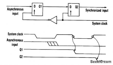
This common synchronization method uses two rippled 74LS74 D-type flip-flops. (View)
View full Circuit Diagram | Comments | Reading(802)
SYNC_TIP_dc_RESTORER
Published:2009/6/24 3:26:00 Author:May
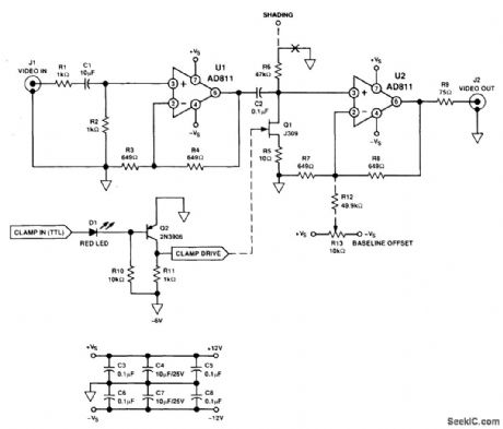
The dc restorer shown supplies a video signal with sync tips clamped to a baseline level. Clamp drive signal is supplied from elsewhere, usually a sync generator or a sync separator. (View)
View full Circuit Diagram | Comments | Reading(0)
| Pages:11/24 1234567891011121314151617181920Under 20 |
Circuit Categories
power supply circuit
Amplifier Circuit
Basic Circuit
LED and Light Circuit
Sensor Circuit
Signal Processing
Electrical Equipment Circuit
Control Circuit
Remote Control Circuit
A/D-D/A Converter Circuit
Audio Circuit
Measuring and Test Circuit
Communication Circuit
Computer-Related Circuit
555 Circuit
Automotive Circuit
Repairing Circuit