
Analog Circuit
Index 4
The adjustable Pulse signal source circuit with frequency and pulse width(CD4011)
Published:2011/8/4 8:10:00 Author:nelly | Keyword: Pulse, signal source, frequency, pulse width
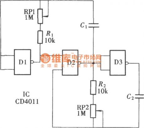
The signal pulse width of the general pulse generator will change with the oscillation frequency, when it is changing its oscillation frequency. Conversely, when the pulse needs to be changed, the oscillation frequency will also change. This circuit can make the pulse width of the pulse and the frequency change independently, so they will not influence each other, the circuit is as shown..
The table of oscillation frequency and pulse width:
(View)
View full Circuit Diagram | Comments | Reading(870)
CALCULATOR_KEYBOARD_ENTRY_
Published:2009/7/12 21:25:00 Author:May
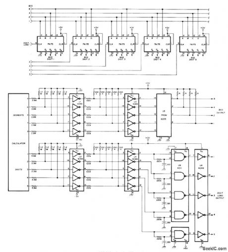
Sampling of signals from inexpensive pocket calculator gives complete data entry system for frequency synthesizer or other application requiring BCD input. Circuit includes contact bounce suppression. Automatic constant feature of TI 1256 calculator used permits storing 0.015 as fixed constant, so frequency goes up 15 kHz (channel spacing on 2 meters) each time + key is pressed.Seven-segment signal normally used for calculator display is decoded by programming 74S188 (8223) PROM, using simplified code conversion table given in article. 74175 ICs provide required demultiplexing of segment data. Articl gives construction details.-B .McNair andG Williman,Digital Keyboard Entry System,Ham Radio, Sept,1978,p 92-97.
(View)
View full Circuit Diagram | Comments | Reading(3694)
SINE_WAVE_SQUARE_WAVE_CONVERTER
Published:2009/7/10 2:07:00 Author:May
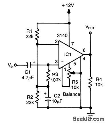
An op amp used as a comparator produces a 10-V p-p square-wave output with 100-mV input, to 15 kHz. Adjust R5 for symmetry of square wave at low input levels. (View)
View full Circuit Diagram | Comments | Reading(3246)
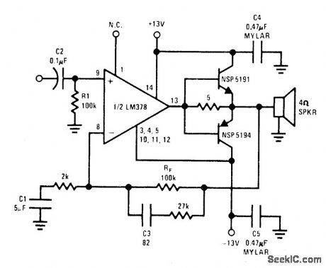
DERIVED_CENTER_CHANNEL_STEREO_SYSTEM
Published:2009/7/9 1:48:00 Author:May
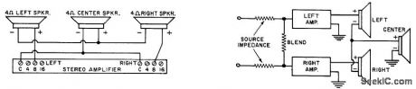
A simple method of deriving a center or third channel without the use of an extra transformer or amplifter. (a) 4-Ω speakers are connected to 8-Ω amplifier taps. 8 and 16-Ω speakers connect to 16-Ω taps. (b) By blending the inputs it is possible to cancel out undesired crosstalk. (View)
View full Circuit Diagram | Comments | Reading(1099)
ANALOG_MULTIPLEXER_WITH_BUFFERED_INPUT_AND_OUTPUT
Published:2009/7/8 22:01:00 Author:May
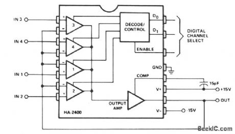
This circuit is used for analog signal selection or time division multiplexing. As shown, the feedback signal places the selected amplifier channel in a voltage follower (noninverting unity gain) configuration, and provides very high input impedance and low output impedance. The single package replaces four input buffer amplifiers, four analog switches with decoding, and one output buffer amplifier. For low-level input signals, gain can be added to one or more channels by connecting the (-) inputs to a voltage divider between output and ground. The bandwidth is approximately 8 MHz, and the output will slew from one level to another at about 15.0 V per μs.
Expansion to multiplex 5 to 12 channels can be accomplished by connecting the compensation pins of two or three devices together, and using the output of only one of the devices. The enable input on the unselected devices must be low.
Expansion to 16 or more channels is accomplished easily by connecting outputs of four 4-channel multiplexers to the inputs of another 4-channel multiplexer. Differential signals can be handed by two identical multiplexers addressed in parallel. Inverting amplifier configurations can also be used, but the feedback resistors might cause crosstalk from the output to unselected inputs.
(View)
View full Circuit Diagram | Comments | Reading(1991)
T_ATTENUATOR_
Published:2009/7/8 4:22:00 Author:May
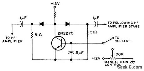
When inserted between stages of IF amplifier, circuit acts as three.section attenuator with dynamic range greater than 60 dB. Can be controlled by positive voltage from AVC system of receiver or manually with 100K pot. Use PIN diodes.-Super Circuits, 73 Magazine, Aug. 1975, p 140. (View)
View full Circuit Diagram | Comments | Reading(1016)
PULSE_AMPLITUDE_DISCRIMINATOR
Published:2009/7/8 2:15:00 Author:May
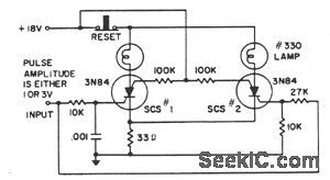
A 1-V amplitude pulse triggers SCS1,but has insufficient amplitude to trigger SCS2.A 3-V mputpulse is delayed h reaching SCS1 by the 10-KΩ and.001-μF integrating network.Instead,it triggers SCS2,then ralses the common emitter voltage to prevent SCS1 from triggering.The 100-KΩ resistors Suppress the rate effect. (View)
View full Circuit Diagram | Comments | Reading(1)
CLOSED_LOOP_TRACER
Published:2009/7/8 2:13:00 Author:May
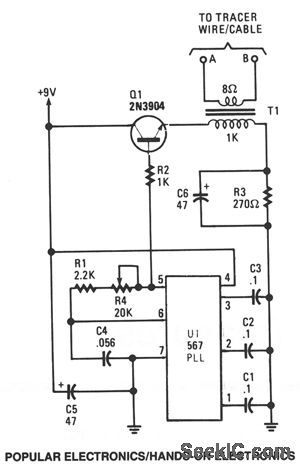
The tracer, consisting of both a transmitter and receiver, is designed to follow a closed-loop wire or cable system. It follows an induced voltage path created by feeding a low-current, audio-frequency signal through the cable. When the pick-up coils come within close proximity of the current-carrying cable, a small voltage is generated in each coil, and that induced voltage is then processed by the receiver's circuitry.
The circuit is built around a 567 phase-locked loop (PLL) configured as a variable-frequency, audio-generator circuit, which is designed to produce a square-wave output at pin 5. Potentiometer R4 allows the oscillator to be easily tuned to the receiver's frequency. Transistor Q1 isolates the oscillator from the load and matches the impedance of the primary of T1. Resistor R3 limits current flow through Q1. The low-impedance secondary of T1 supplies the cable drive signal. (View)
View full Circuit Diagram | Comments | Reading(3500)
ANALOG_SUMMING
Published:2009/7/7 5:24:00 Author:May
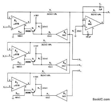
ON/OFF programming ofμA776 opamps allows any or all inputs to be on at given time. Switched outputs are combined in summing inverter A,. Voltage followers A1-A3 are programmed from on to off by Q1-Q3 and A5- A7. Noise gain of stage A4, is minimized when input channel is switched off. If sign inversion by A4, is undesirable, add inverter stage following A.. Any number of additional channels can be added. Programming pulses are applied to inputs of A,, A6, and A,.-W. G. Jung, IC 0p-Amp Cookbook, Howard W Sams, Indianapolis, IN, 1974, p 419-421. (View)
View full Circuit Diagram | Comments | Reading(793)
VOLTAGE_DETECTOR_RELAY_FOR_BATTERY_CHARGER
Published:2009/7/3 4:21:00 Author:May
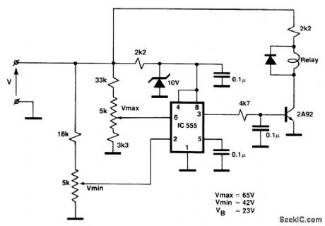
While the battery is being charged, its voltage is measured at V. If the measured voltage is lower than the minimum the relay will be energized, that will connect the charger circuit. When the battery voltage runs over the maximum set point, the relay is deenergized and it will be held that way until the voltage decreases below the minimum when it will be connected again. The voltage is lower than a threshold VB (low breaking voltage) the relay will be assumed that such a low voltage is due to one or several dam-aged battery components. Of course VB is much lower than the minimum set point. (View)
View full Circuit Diagram | Comments | Reading(1003)
2258_Hz_REJECTION
Published:2009/7/2 23:45:00 Author:May
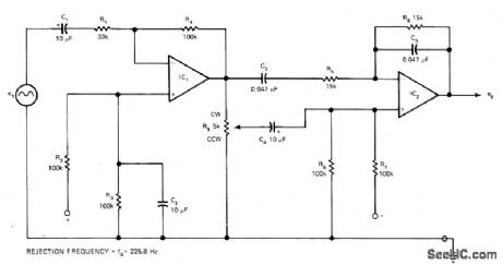
Provides extremely sharp adjustable-depth notch with only two low-gain opamps. Suitable for single-ended supplies. Article gives equation for transfer function.-R. Carter, Sharp Null Filter Utilizes Minimum Component Count, EDN Magazine, Sept. 20, 1976, p 110.
(View)
View full Circuit Diagram | Comments | Reading(689)
LITTLE_DIPPER
Published:2009/7/1 22:03:00 Author:May
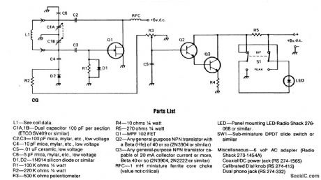
The circuit consists of two basic circuits, the oscillator and the detector. The oscillator uses an FET in a Colpitts configuration. The energy circulating in the oscillator tank is coupled through C4 to the detector circuit, where a small diode (D2) rectifies it, feeding a dc voltage to the Darlington pair (Q2, A3) con-trolled by the sensitivity control (R3). Any smallvariations in the bias of the amplifier will cause large variations of current through the LED indicator in the DiP mode; however, in the PEAK mode the current produces a corre-sponding voltage ropthrough R5 and the action of the LED is reversed. The circuit shown will work practically on any frequency from LF to VHF if the appropriate components are used. (View)
View full Circuit Diagram | Comments | Reading(958)
ALARM_FOR_SPECTRUM_ANALYZER
Published:2009/7/1 21:21:00 Author:May
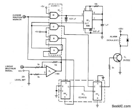
Circuit drives audible alarm when frequency of interest appears in spectrum range. Display cursor can be preset to initiate narrow search band in which fx is expected to appear. 100-μs pulse representing cursor position in display sweep triggers mono IC1 so its output becomes window whose time-out is equivalent to band in which fx is center. Comparator A1 supplies high output when fx appears. Simultaneous arrival of this signal and timer window at gate A sets output of left flip-flop high. At end of window period, right flip-flop also goes high and initiates alarm via Q1. Loss of fX stops alarm.-R. L. Messick, Alarm Simplifies Spectrum-Analyzer Measurements, EDN Magazine, JuneS, 1978, p 152. (View)
View full Circuit Diagram | Comments | Reading(885)
6_BITS_TO_ANALOG
Published:2009/6/30 2:59:00 Author:May
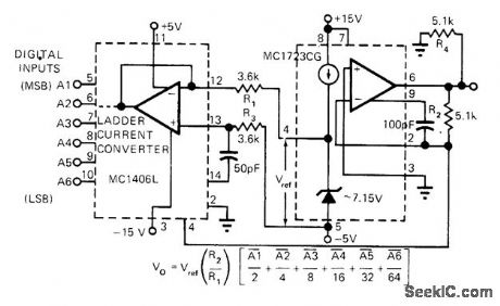
Uses Motorola MC1723G voltage regulator to provide reference voltage and opamp for MC1406L 6-bit D/A converter. Output cument can be up to 150 mA. Full-scale output is about 10 V, but can be boosted as high as 32V by increasing value of R2 and increasing +15 V supply proportionately to maximum of 35 V.—D. Aldridge and K. Huehne, 6-Bit D/A Converter Uses Inexpensive Components, EDN Magazine, Dec. 15, 1972, p 40-41. (View)
View full Circuit Diagram | Comments | Reading(796)
0_10_V_ANALOG_INPUT
Published:2009/6/30 1:25:00 Author:May
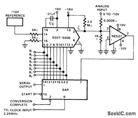
Used to provide digital input to computer for processing and storage of analog signals. Requires only three ICs in addition to external +10 V reference and 2.25-MHz TTL clock. Successive-approximation register (SAR) can be Motorola MC1408 or equivalent. For continuous conversions, connect pins 10 and 2 of SAR.— Signetics Analog Data Manual, Signetics, Sunnyvale, CA, 1977, p 677-685. (View)
View full Circuit Diagram | Comments | Reading(1595)
HIGH_GAIN_JFET
Published:2009/6/29 2:38:00 Author:May
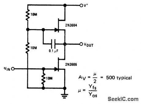
Simpletwo-JFET circuit provides gain of 500 at low power. Reducing drain cument increases gain at sacrifice of input dy-namic range.- FET Databook, National Semi-conductor, Santa Clara, CA, 1977, p 6-26-6-36. (View)
View full Circuit Diagram | Comments | Reading(1004)
FIBER_OPTIC_RECEIVER,LOW_SENSITIVITY,2μW
Published:2009/6/29 2:08:00 Author:May

View full Circuit Diagram | Comments | Reading(622)
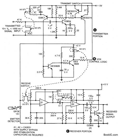
FIBER_OPTIC_LINK
Published:2009/6/29 2:04:00 Author:May
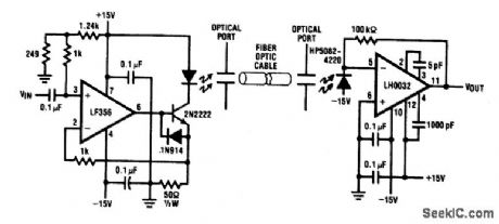
Circuit Notes
Fiber Optic applications require analog drivers and receivers operating in the megahertz region. This complete analog transmission system is suitable for optical communication applications up to 3.5 MHz.The transmitter LED is normally biased at 50 mA operating current. The input is capacitively coupled and ranges from 0 to 5 \I, modulating the LED current from 0 to 100 mA. The re-ceiver circuit is configured as a transimpe-dance amplifier. The photodiode with 0.5 amp per watt responsivity generates a 50 mV signal at the receiver output for 1,u,W of light input. (View)
View full Circuit Diagram | Comments | Reading(2)
FIBER_OPTIC_RECEIVER,VERY_HIGH_SENSITIVITY,LOW_SPEED,3nW
Published:2009/6/29 2:00:00 Author:May
View full Circuit Diagram | Comments | Reading(640)
FIBER_OPTICS_HALF_DUPLEX_INFORMATION_LINK
Published:2009/6/29 1:58:00 Author:May
View full Circuit Diagram | Comments | Reading(701)
| Pages:4/24 1234567891011121314151617181920Under 20 |
Circuit Categories
power supply circuit
Amplifier Circuit
Basic Circuit
LED and Light Circuit
Sensor Circuit
Signal Processing
Electrical Equipment Circuit
Control Circuit
Remote Control Circuit
A/D-D/A Converter Circuit
Audio Circuit
Measuring and Test Circuit
Communication Circuit
Computer-Related Circuit
555 Circuit
Automotive Circuit
Repairing Circuit