
Analog Circuit
Index 14
LOW_POWER_dc_DOUBLER
Published:2009/6/23 5:02:00 Author:May
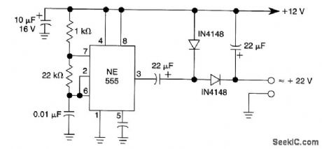
This dc voltage-doubler circuit based on the 555 can produce a dc output voltage equal to ap-proximately 2× the dc supply voltage. (View)
View full Circuit Diagram | Comments | Reading(2001)
LOW_POWER_dc_QUADRUPLER
Published:2009/6/23 5:01:00 Author:May
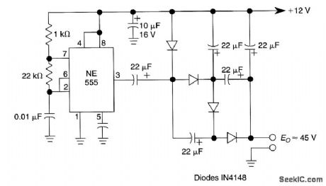
This dc voltage-quadrupler circuit based on the 555 can produce a dc output voltage equal to ap-proximately 4×the dc supply voltage. (View)
View full Circuit Diagram | Comments | Reading(3060)
PULSE_WIDTH_MODULATOR
Published:2009/6/23 5:00:00 Author:May
View full Circuit Diagram | Comments | Reading(1)
LOW_POWER_dc_TRIPLER
Published:2009/6/23 5:00:00 Author:May
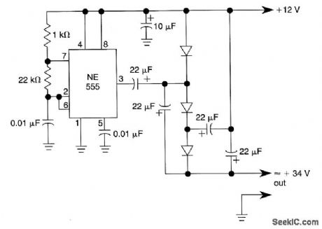
This dc voltage-tripler circuit based on the 555 can produce proximately 3× the dc supply voltage. (View)
View full Circuit Diagram | Comments | Reading(4191)
FOUR_QUADRANT_MULTIPLIER_AS_DSB_MODULATOR
Published:2009/6/23 4:57:00 Author:May
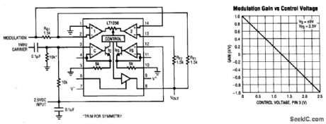
View full Circuit Diagram | Comments | Reading(756)
DIGITAL_PULSE_WIDTH_MODULATION_CIRCUIT
Published:2009/6/23 4:54:00 Author:May
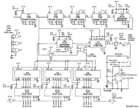
This circuit incorporates low-power Schottky transistor/tr ansistor-lo gic (TTL) devices in critical high-speed parts. The 5-MHz clock signal is converted to a 1-MHz signal by a 7490 decade counter configured to divide by 5. The 1-MHz signal is sent, via a clock synchronizer, to a three-stage binary divider that consists of three cascaded 74LS161 binary dividers. The synchronizer consists of a 74LS74 D flip-flop, a 7404 inverter gate, and a 7402 NOR gate. The dividers are programmed from the STD bus by means of three 7475 quad latches; this makes it possible to program the frequency divi-sion from 1 to 4096 (12 bits).The 1-MHz signal is also divided by 1000 by use of three cascaded 7490 decade counters, each configured to divide by 10; this provides a 1-kHz signal, which is sent to a 54121 monostable multivi-brator configured to provide a 0.1-ps pulse, bombarded with an ion beam source in preparation for the materials about to be deposited. While the surface is bombarded with an ion beam, an electron beam source is activated so that a layer of fused silica is vapor-deposited to a total desired thickness value (typically, 1 micron or t0,000 A). The layer offused silica serves as a surface stabilization layer for the next step.A metal mask with an aperture in the specified pattern of the sensor film is placed on the surface at the specified sensor location. The surface area exposed through the mask is cleaned by ion-beam bombardment for a predetermined time. Then as the bombardment continues, a metal (typically, nickel, platinum, and/or palladium) is vapor-deposited through the mask from the electron-beam source to form the sensor film. Deposition is continued until the thickness of the film reaches the value specified in the particular sensor design. A representative value for a nickel sensor film is 2500 A.Next, a pattern for thin film leads is defined by taping directly on the surface of the model with Kapton (or equivalent) polyimide tape. The thin film leads are fabricated by a combination of ion-beam bombardment and electron-beam vapor deposition like that used to deposit the sensor film.The metal vapor deposited in this step is typically copper, gold, or aluminum. A typical thickness for copper leads on the nickel sensor film is about 10,000 A. (View)
View full Circuit Diagram | Comments | Reading(3069)
TWO_PHASE_RECTIFIER
Published:2009/6/23 4:21:00 Author:May
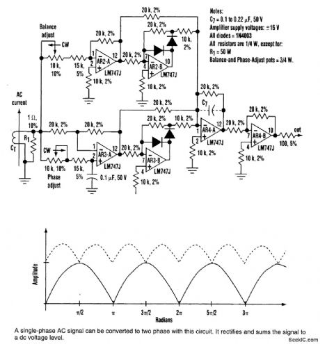
The waveform generated by the two-phase rectifier illustrates that the ripple is less than half that of a conventional single-phase circuit's wavefrom. Also,the ripple frequency is double that of the conventional circuit. The circuit amplitude changes in the ac input signal very rapidly,and it works equally will with current or voltage inputs. (View)
View full Circuit Diagram | Comments | Reading(843)
REGULATOR_CIRCUIT_FOR_BILATERAL_SOURCE_LOAD_POWER_SYSTEM
Published:2009/6/23 4:10:00 Author:May
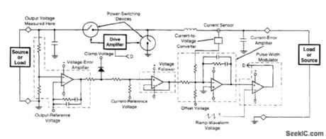
The figure shows a circuit that regulates an output voltage, regardless of the direction of flow of output current. More specifically, it regulates the voltage at the left source or load, which can either supply power to or receive power from the right load or source, depending on the voltages and the direction of flow of current at the load/source terminals.The overall system can be characterized as a voltage-controlled current source with bilateral current capability. The current flowing between the two source/loads, averaged over a power-switching cycle, is made to depend on the pulse-width modulation that governs the operation of the two power-switching devices, and this pulse-width modulation is, in turn, a function of amplified currenterror and voltage-error signals. The voltage error is the difference between the actual output voltage and the output-reference voltage, which is the nominal output voltage at zero current. The pulsewidth modulation is varied to increase or decrease the current, as needed, to limit the excursion of output voltage from the reference value.An additional feature of this control circuit is that the maximum current in either direction can be limited by limiting the excursion of the output voltage from the zero-current value. Thus, external current-limiting circuitry is not necessary. (View)
View full Circuit Diagram | Comments | Reading(719)
VARACTORLESS_HF_MODULATOR
Published:2009/6/23 4:36:00 Author:May
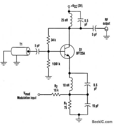
Traditionally, high-frequency oscillators are frequency-modulated by using a varactor. However, varactors usually require a large voltage change to achieve a reasonable capacitance change-a prob-lem in many battery-powered systems.Such a problem can be overcome by employing base-charging capacitance modulation. Resistor RI establishes Q1's current, and R2 allows control of the collector bias current byVmod The trans-mission line (T1) in the negative resistance-type oscillator determines the frequency of oscillation. T1 is a high-quality, low-loss, ceramic coaxial shorted quarter-wave transmission line. Under proper terminal impedances, a negative resistance is seen at Q1's base. T1 reacts with this negative resis-tance to produce sustained oscillations.Frequency modulation is accomplished by changing Q1's collector bias current and thus chang-ing Q1's base-charging capacitance. This effect is seen at Q1's base and causes a frequency shift in the resonators quarter-wave node. (View)
View full Circuit Diagram | Comments | Reading(0)
VIDEO_MASTER
Published:2009/6/23 3:58:00 Author:May

The video master consists of a series of converters that place all your video sources on unused UHF channels, which then combines them with normal TV channels (terrestrial or cable into one ca-ble). That one cable can then feed several TV sets for whole-house coverage. The desired video source is selected with the TV set's tuner. All of the TV's remote-control features are retained.A complete kit of parts is available from North Country Radio, P.O. Box 53, Wykagyl Station, New Rochelle, NY 10804-0053A. (View)
View full Circuit Diagram | Comments | Reading(0)
FAST_33_V_REGULATOR
Published:2009/6/23 3:45:00 Author:May
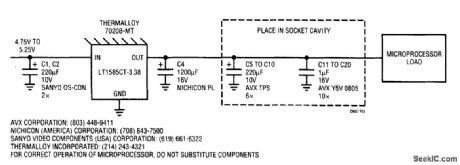


New high-performance microprocessors require a fresh look at power-supply transient response.The LT1585 linear regulator features 1% initial accuracy, excellent temperature drift and load regulation, and virtually perfect line regulation. Complementing superb dc characteristics, the LT1585 exhibits extremely fast response to transients. Transient response is affected by more than the regulator itself. Stray inductances in the layout and bypass capacitors, as well as capacitor ESR dominate the response during the first 400 ns of transient.The ftgure shows a bypassing scheme developed to meet all the requirements for the Intel P44C-VR microprocessor. Input capacitors C1 and C2 function primarily to decouple load transients from the 5-V logic suppJy. The values used here are optimized for a typical 5-V desktop computer silver box powersupply input. C5 to C10 provide bulk capacitance at low ESR and ESL, and C11 to C20 keep the capacitance at low ESR and ESL low at high (>100 kHz) frequencies. C4 is a damper and it minimizes ringing during setting. Trace C is the load current step, which is essentially flat at 4 A with a 20-ns rise time.Trace A is the output settling response at 20 mV per division. Cursor trace B marks -46 mV relative to the initial output voltage. At the onset of load current, the microprocessor socket voltage dips to -38 ntV as a result of inductive effects in the board and capacitors, and the ESR of the capacitors. The inductive effects persist for approximately 400 ns. For the next 3 μs, the output droops as the load current drains the bypass capacitors. The trend then reverses as the LT1585 catches up with the load demand, and the output settles after approximately 50 μs. Running 4 A with a 1.7-V drop, the regulator dissipates 6.8 W. (View)
View full Circuit Diagram | Comments | Reading(0)
GROUND_LOOP_PREVENTER
Published:2009/6/23 3:32:00 Author:May
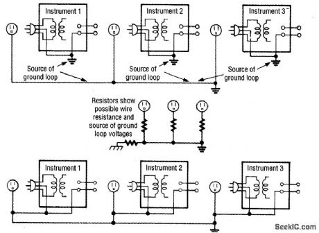
Ground loops are caused by improper grounding. Ground-loop voltages can interfere with test rrteasurements because the voltages in a ground loop can be larger than the signals you're trying to measure. To prevent ground loops, use two wire plugs to provide the line power to the test instru-ments and a separate wire to bring the input grounds of the instruments to a common ground. (View)
View full Circuit Diagram | Comments | Reading(0)
JACOB’s_LADDER
Published:2009/6/23 3:28:00 Author:May
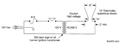
A“Iacobs Ladder”can be made from an old neon sign or oil burner ignition transformer. A rating of 12 to 15 kV at 20 to 30 mA will be adequate. Make sure to mount the electrodes to a pair of in-sulators, at least 2 apart, and bent and spaced, as shown. The ladder should be enclosed in a clear plastic housing to prevent accidental contact with the high voltage and to ensure a stable arc. Vent holes should be placed top and bottom to allow gases to escape. (View)
View full Circuit Diagram | Comments | Reading(2776)
×10_FREQUENCY_MULTIPLIER
Published:2009/6/23 3:23:00 Author:May
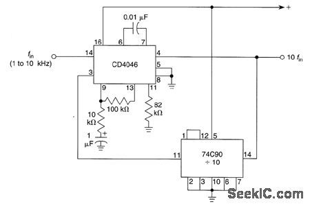
In this circuit, the CD4046 is set up so that the VCO operates at 10 to 100 kHz. The output pin(4) is fed back to a ÷10 counter. When the input frequency is 1/10 the output, lockup will occur. (View)
View full Circuit Diagram | Comments | Reading(3171)
POSITIVE_FEEDBACK_CABLE_TERMINATOR
Published:2009/6/23 3:18:00 Author:May
Positive feedback along with a series output resistor can provide a controlled output impedance from an op-amp circuit. The circuit is useful when driving coaxial cables that must be terminated at each end in their characteristic impedance, which is often 50Q. Adding a 50-Q series resistor on the op amp's output obviously reduces the available signal swing. (View)
View full Circuit Diagram | Comments | Reading(0)
455_kHz_MODULATOR
Published:2009/6/23 3:10:00 Author:May
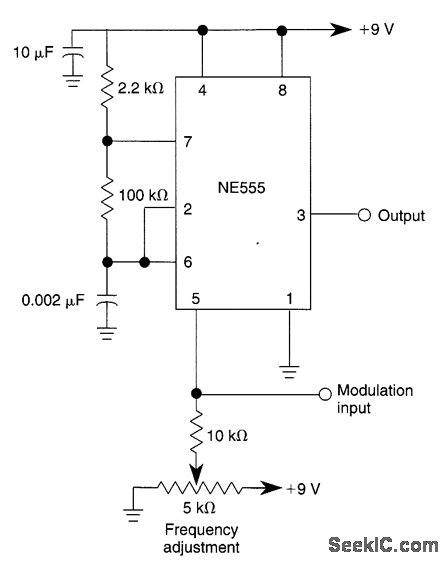
This circuit shows how to frequency-modutate the oscillator using a 555. Oscillator frequency is set with the 5-kΩ potentiometer and the modulation signal is dc-coupled. (View)
View full Circuit Diagram | Comments | Reading(0)
FM_MODULATOR
Published:2009/6/23 3:08:00 Author:May
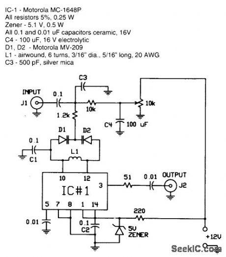
The FM modulator is built with a Motorola MC1648P oscillator. Two varactors, Motorola MV209, are used to frequency modulate the oscillator. The 5000-Ω potentiometer is used to bias the varactors for best linearity. The output fre-quency of approximately 100 MHz can be ad-justed by changing the value of the inductor. The output frequency can vary as much as 10 MHz on each side. The output level of the modulator is -5 dBm. In this prototype, the varactor bias was 7.5 V for best linearity; but this could be different with other varactors. (View)
View full Circuit Diagram | Comments | Reading(0)
UNITY_GAIN_FOUR_INPUT_AUDIO_MIXER
Published:2009/6/23 3:02:00 Author:May
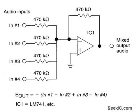
The circuit has four inputs. The voltage gain between each input and the output is held at unity by the relative values of the 470kΩ input resistor and the 470kΩ feedback resistor. (View)
View full Circuit Diagram | Comments | Reading(1107)
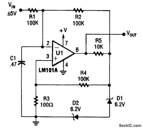
PRECISION_AVSOLUTE_VALUR_CIRCUIT
Published:2009/6/23 3:02:00 Author:May
View full Circuit Diagram | Comments | Reading(630)
CONTACT_DEBOUNCER
Published:2009/6/23 3:00:00 Author:May
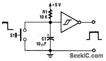
A contact debouncer using a Schmitt trigger, such as a TTL7414, provides a clean pulse from a switch contact closing. (View)
View full Circuit Diagram | Comments | Reading(777)
| Pages:14/24 1234567891011121314151617181920Under 20 |
Circuit Categories
power supply circuit
Amplifier Circuit
Basic Circuit
LED and Light Circuit
Sensor Circuit
Signal Processing
Electrical Equipment Circuit
Control Circuit
Remote Control Circuit
A/D-D/A Converter Circuit
Audio Circuit
Measuring and Test Circuit
Communication Circuit
Computer-Related Circuit
555 Circuit
Automotive Circuit
Repairing Circuit