
Analog Circuit
Index 12
VOLTAGE_TRIPLER_FOR_RADONDETECTOR_IONIZATION_CHAMBER
Published:2009/6/24 3:22:00 Author:May
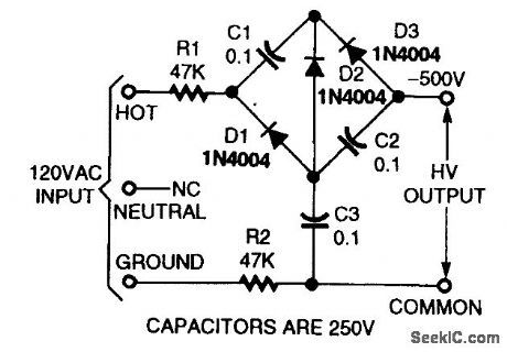
The voltage tripler charges the ionization chamber capacitor. It is powered from the 120-Vac line. Warning: Shock hazard exists. (View)
View full Circuit Diagram | Comments | Reading(1167)
SWITCH_ON_DELAY_CIRCUIT
Published:2009/6/24 3:19:00 Author:May
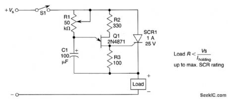
When S1 is tumed on, a very small current flows through the load. Almost the entire supply volt-age appears across the SCR. When C1 changes up to the firing voltage of Q1 (approximately the standoff ratio of Q1 times VS, usually 0.4 to 0.6 VS) through R1, Q1 fires, tuming on SCR1. This deliv-ers full voltage to load, minus SCR drop (about 1.2 V). Notice that load current must exceed SCR holding current. (View)
View full Circuit Diagram | Comments | Reading(897)
POLARITY_PROTECTOR
Published:2009/6/24 3:13:00 Author:May
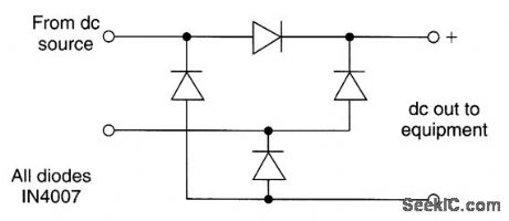
The use of a four-diode bridge guarantees correct polarity irrespective of input dc polarity. Remember that two diode drops (about 1.2 to 1.5 V) are lost from the input voltage using this circuit (View)
View full Circuit Diagram | Comments | Reading(902)
SHORT_CIRCUIT_PROTECTION_CIRCUIT
Published:2009/6/24 3:11:00 Author:May
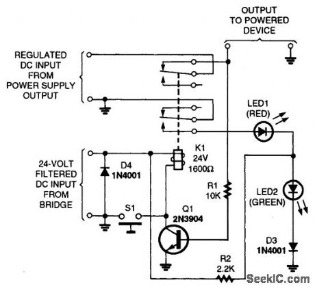
When S1 is pressed, the coil of K1 is energized, closing its norrrtally open contacts. If the regulated dc input is between 1 and 24 V, that voltage feeds the base of Q1 through R1, turning on the transistor, and latching the relay. When that occurs, LED2 glows indicating that all is okay.If there is a short to ground at the circuit's output (i.e., in the device being powered), the voltage that feeds the base of Q1 goes to zero, turning off the transistor. Then, LED1 glows because K1 is de-energized to indicate the short circuit. (View)
View full Circuit Diagram | Comments | Reading(1079)
NOVEL_LOUDSPEAKER_COUPLING_CIRCUIT
Published:2009/6/24 3:11:00 Author:May
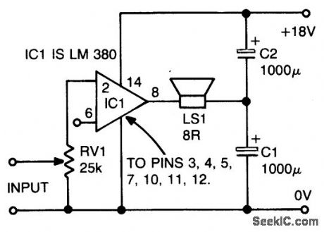
The ground side of the speaker is con-nected to the junction of two equal high value capacitors (1000 μF is typical) across the sup-ply. The amplifier output voltage will be VS/2, and so will the voltage across C1 (if C1 and C2 are equal); so as the supply voltage builds up, the dc voltage across the speaker will remain zero, eliminating the switch-on surge. C1 and C2 will also provide supply smoothing. The circuit is shown with the LM380, but could be applied to any amplifier circuit, providing that the dc voltage at the output is half the supply voltage. (View)
View full Circuit Diagram | Comments | Reading(896)
8_DIGIT_100_MHz_FREQUENCY_PROBE
Published:2009/6/24 3:10:00 Author:May
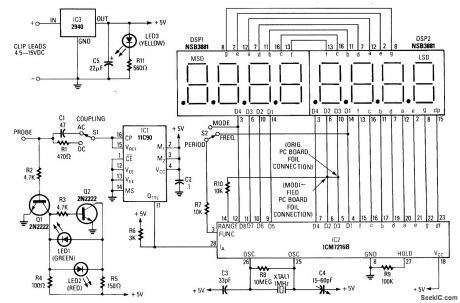
Small enough to mount in a probe, this frequency counter circuit is good to 100 MHz. It operates from +5 to +15 Vdc. An 11C90 prescaler drives a 10-MHz counter chip (ICM7216B). Note the dotted line connecting R10 with pins 5 and 6 of IC2; that variable connection controls the decimal point and total count appearing on DSP1 and DSP2. The relative intensities and dura-tions of ON/OFF time for LED1 (green) and LED2 (red) give a rough indication of logic level and duty cycle. (View)
View full Circuit Diagram | Comments | Reading(8140)
OSCILLATOR_TRIGGERED_SWITCH
Published:2009/6/24 3:09:00 Author:May
In this circuit (the oscillator-triggered switch), the generated by an astable oscillator. (View)
View full Circuit Diagram | Comments | Reading(0)
LOW_OUTPUT_IMPEDANCE_MULTIPLEXER
Published:2009/6/24 3:08:00 Author:May
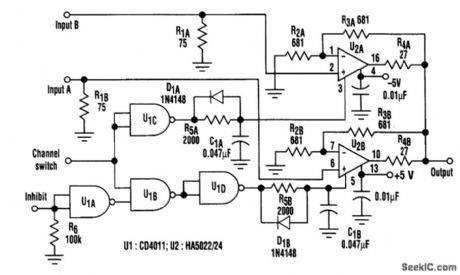
Both inputs are terminated in their characteristic impedance; 75Ω is typical for video applications. Because the output cables usually are terminated in their characteristic impedance, the gain is 0.5. Consequently, amplifiers U2A and U2B are configured in a gain of +2 to set the circuit gain at 1.R2 and R3 determine the amplifier gain; if a different gain is desired, R2 should be changed according to the equation G = (1 + R3/R2) R5, LCL1, and D1 make up an asymmetrical charge/discharge time circuit that configures U1 as a break-before-make switch to prevent both amplifiers from being ac-tive simultaneously. The multiplexer transition time is approximately 15μs with the component values shown. (View)
View full Circuit Diagram | Comments | Reading(0)
ANALOG_SWITCH_CIRCUIT
Published:2009/6/24 3:05:00 Author:May
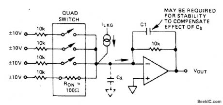
View full Circuit Diagram | Comments | Reading(849)
ANALOG_SWITCHED_INVERTER
Published:2009/6/24 3:05:00 Author:May
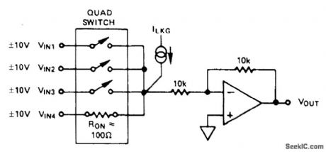
View full Circuit Diagram | Comments | Reading(653)
SIMPLE_LOGIC_PROBE_WITH_ALPHANUMERIC_DISPLAY
Published:2009/6/24 3:03:00 Author:May
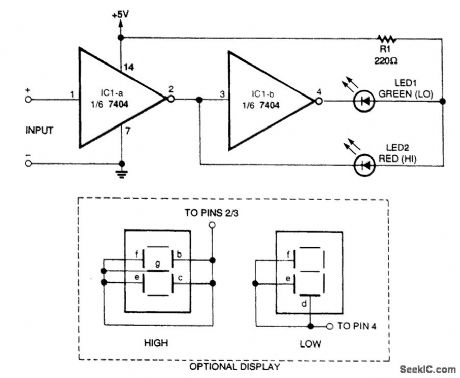
A logic probe also includes BCD decoder module. The red LED lights to indicate a logic high, and the green LED lights to indicate a logic low. This probe circuit will light a green (low) or red (high), and if desired, an alphanumeric display can be obtained with two 7-segment LED displays. (View)
View full Circuit Diagram | Comments | Reading(2200)
STEPPER_MOTOR_ENCODER_CIRCUIT
Published:2009/6/24 3:00:00 Author:May
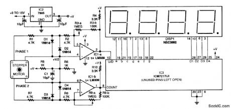
This circuit translates shaft rotation and direction to a readout on an LED display. A stepper motor is used as an encoder. (View)
View full Circuit Diagram | Comments | Reading(0)
ADJUSTABLE_BIAS_REGULATOR
Published:2009/6/24 2:59:00 Author:May
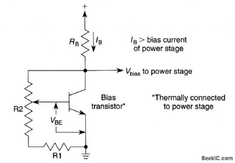
If the wiper of R2 is set at N% rotation,the bias voltage Will be∶This method derives a bias voltage that tracks VBE of this bias transistor. If the bias transistor is thermally linked to the power stage, tracking over a wide temperature range will result. (View)
View full Circuit Diagram | Comments | Reading(0)
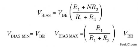
STEPPER_MOTOR_AS_SHAFT_ENCODER
Published:2009/6/24 2:59:00 Author:May
To use a stepper as a shaft encoder, the out-put signals must be converted to square waves with a pair of voltage comparators. (View)
View full Circuit Diagram | Comments | Reading(0)
ADJUSTABLE_POSITIVE_REGULATOR
Published:2009/6/24 2:57:00 Author:May
View full Circuit Diagram | Comments | Reading(0)
POLARITY_GAIN_ADJUSTMENT
Published:2009/6/24 2:53:00 Author:May
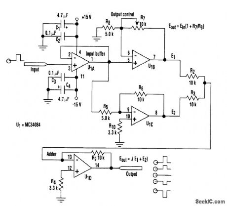
By adjusting one potentiometer, this circuit's output can be varied from a positive-going version of the input signal, smoothly through zero output, then to a negative-going version of the input (see the figure). If the input signal is a positive pulse of, for example, +2-V peak, the output pulse amplitude can be smoothly varied from +2-V through ground (no output) to a -2-V peak.
Taking a closer look at the setup, assume that the signal has a +2-V peak input. The A section of the quad op amp is an input buffer, op amp C provides a fixed negative-going output of -4-V peak, and op amp B supplies a positive-going output that varies from +2-V to +6-V peak. The D section adds the B and C outputs. Thus, by varying the B output, the circuit output varies smoothly from -2-V to +2-V peak.
The circuit can, of course, also be used as a 0°/180° phase switcher. For instance, with a groundcentered sine-wave input of 4V p-p, the output varies from 4-V p-p in phase with the input, smoothly through 0 V, to 4V p-p 180° out of phase with the input. (View)
View full Circuit Diagram | Comments | Reading(882)
SHARP_SQUARE_WAVEFORMS_FROM_MULTIVIBRATOR
Published:2009/6/24 2:50:00 Author:May
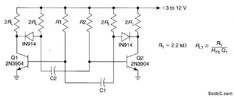
By using diodes as shown, the loading effect on the collector of the transistors caused by the tim-irtg capacitors can be avoided. As the collector of the transistors rises toward VCC the diode discon-nects the tinting capacitors. (View)
View full Circuit Diagram | Comments | Reading(0)
RECEIVER_AF_NOISE_LIMITER_FOR_LOW_LEVEL_SIGNALS
Published:2009/6/24 2:46:00 Author:May
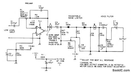
A preamplifier in the audio frequency range amplifies a noisy audio signal to drive a diode clip-per. Suitable audio input levels would be in the 10-mV to 1-V range. (View)
View full Circuit Diagram | Comments | Reading(0)
GUNSHOT_SOUND_EFFECTS_GENERATOR
Published:2009/6/24 2:46:00 Author:May
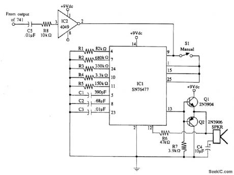
Gunshot sound-effects generator built around a Texas Instruments SN76477 sound chip. An in-put pulse causes IC1 to generate a gunshot sound. (View)
View full Circuit Diagram | Comments | Reading(0)
ELECTRONIC_WIND_CHIME
Published:2009/6/24 2:45:00 Author:May
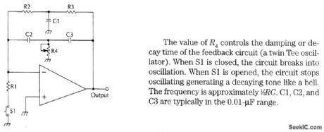
The value of R4 controls the damping or decay time of the feedback circuit (a twin Tee oscillator). When S1 is closed, the circuit breaks into oscillation. When S1 is opened, the circuit stops oscillating generating a decaying tone like a bell.The frequency is approximately 1/2 RC. C1, C2, and C3 are typically in the 0.01-μF range. (View)
View full Circuit Diagram | Comments | Reading(0)
| Pages:12/24 1234567891011121314151617181920Under 20 |
Circuit Categories
power supply circuit
Amplifier Circuit
Basic Circuit
LED and Light Circuit
Sensor Circuit
Signal Processing
Electrical Equipment Circuit
Control Circuit
Remote Control Circuit
A/D-D/A Converter Circuit
Audio Circuit
Measuring and Test Circuit
Communication Circuit
Computer-Related Circuit
555 Circuit
Automotive Circuit
Repairing Circuit