
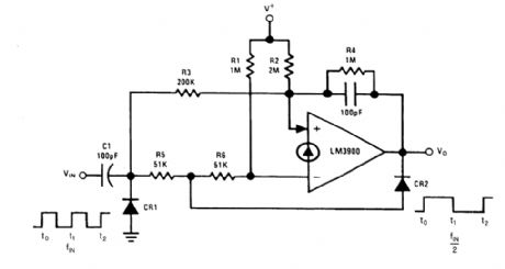
Analog Circuit
Index 18
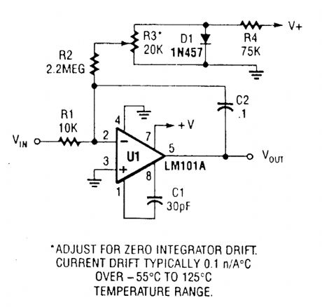
INTEGRATOR_WITH_BIAS_CURRENT_COMPENSATION
Published:2009/6/19 4:39:00 Author:May
View full Circuit Diagram | Comments | Reading(2)
FOUR_INPUT_MINIMUM_MAXIMUM_SELECTOR
Published:2009/6/19 4:34:00 Author:May
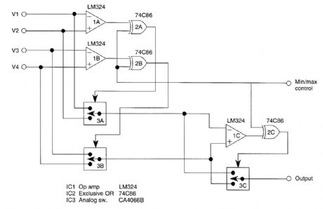
This circuit outputs the maximum (or the minimum) of the four input voltages V1, V2, V3, and V4. Each of these input voltages is in the range 0 to 5V.
The output of the unit is the maximum of V1, V2, V3, and V4 if the control voltage input is 5V (i.e., logical 1). The output is the minimum of V1, V2, V3, and V4 if the control input is zero.
By cascading N such units, one can select the maximum (or the minimum) of 3N + 1 input voltages.
Thus if k is the number of input voltages, we need [(k+1)/3] units. (View)
View full Circuit Diagram | Comments | Reading(889)
4_TO_20_mA_PROCESS_CONTROLLER
Published:2009/6/19 4:27:00 Author:May
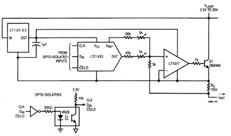
The figure shows how to use an LTC1453 to make an optoisolated digitally controlled 4-to 20-mA process controller. The controller circuitry, including the optoisolator, is powered by the loop voltage that can have a wide range of 3.3V to 30V. The 1.22-V reference output of the LTC1453 is used for the 4-mA offset current and VOUT is used for the digitally controlled 0-to 16-mA current. RS, is a sense resistor and the LT1077 op amp modulates the transistor Q1 to provide the 4-to 20-mA current through this resistor. The control circuitry consumes well under the 4-mA budget at zero scale. (View)
View full Circuit Diagram | Comments | Reading(1307)
ULTRASONIC_GLEANER
Published:2009/6/19 4:18:00 Author:May
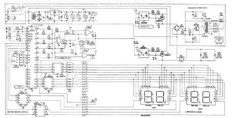
An ultrasonic cleaner is useful to clean certain items. This circuit uses a microcontroller to con-trol timing and give a digital readout, but only the basic oscillator can be used, if desired. RES1, RES2 are piezoelectric transducers driven by power oscillator Q1. Q1 is powered by a bridge rectifier-capacitor input filter that operates directly off the ac line. The frequency is 40 to 60 kHz. (View)
View full Circuit Diagram | Comments | Reading(11260)
VOICE_DISGUISER
Published:2009/6/19 3:20:00 Author:May
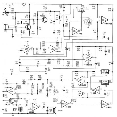
A complete schematic diagram of the voice disguiser is shown. Microphone MIC1 picks up the voice signal and feeds it to an audio amplifier, consisting of Q1 and Q2, and a few support compo-nents. The amplifier has a low-pass gain response that limits the voice frequencies to 5 kHz or lower.
The voice signal is then fed to the input of the first balanced modulator, which is comprised of U1-a, U1-b, U2-a, and U3-a. The output of the first 4-kHz oscillator, built around U3-f and U3-e, is fed to the carrier input of the first modulator. The frequency of the first oscillator is controlled by the setting of potentiometer R13. The modulator output-a double-sideband suppressed-carrier signal centered on 4 kHz-is then filtered by the first 5-kHz low-pass filter, formed by U2-b, which elimi-nates the upper-sideband signals.
At this point, the voice frequency spectrum is inverted (e.g., the frequencies that were low now become high, and vice versa), making the voice signal completely unintelligible. The output of the first low-pass filter is fed to a second modulator formed by U1-c, U1-d, and U3-b, where it is fre-quericy modulated with the output of the second carrier oscillator, comprised of U3-c and U3-d; the frequency of the second oscillator is controlled by potentiometer R36.
The output of the second modulator is filtered by the second low-pass filter, which consists of U2-d and few support components, and amplified by Q3. The voice output signal from Q3 is fed to U4 (an LM386 low-voltage, audio-power amplifier) through an impedance-matching transformer, T1.The output of U4 is then used to drive SPKR1 (an 8-Ω speaker).
In operation, if both carrier oscillators are set to the same frequency, the voice signal from the speaker will be an exact duplicate of the input signal from the microphone. However, if the frequency of the second oscillator is varied (via R36), the output voice signal also shifts in frequency. That makes the voice reproduced by the speaker sound higher- or lower-pitched than normal. (View)
View full Circuit Diagram | Comments | Reading(1445)
ACCELEROMETERG_METERCIRCUIT
Published:2009/6/19 3:09:00 Author:May
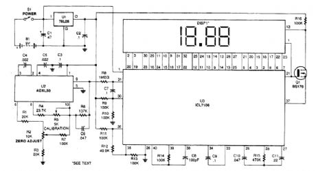
As this schematic shows,the ADXL50 accelerometer,U2,interfaces with an A/D converter,U3, to drive a 3 1/2-digit LCD module, DISPl. Because that module displays any number from -19.99 to +19.99, the circuit is designed to measure g's within that range. The heart of the circuit is U2, the ADXL50 ac-celerometer. The sensitivity of that chip is set to ±20 g's in order to accommodate the full scale capa-bility of LCD module DISP1 (19.99). Circuit gain is determined by the values of R4, R5, and R6, potentiometer R2, and R3 provides a way to manually set the zero-g voltage-output level at pin 9 of U2 to half the supply voltage-2.5V. That output voltage will vary linearly by 0.1-V/g of acceleration.In order to achieve go,od circuit performance at low g levels, the bandwidth of the amplifier is limited to about 30 Hz by C6. The digital-display section of the circuit is composed of DISP1 and U3. Included in U3 are the A/D converter, clock oscillator, storage resistors and latches, 3)6-digit seven-segment decoders, and backplane generator.The differential analog input of U3 is applied between pins 30 and 31. The positive input, pin 31, is driven by output-pin 9 of U2 through R8, a buffer resistor, and the negative input, pin 30, is biased at a fixed voltage of 2.5 V by a voltage-divider string composed of R9 and RIO.A reference voltage is required by U3. Full-scale display, 19.99, occurs when the differential, ana-log input voltage applied between pins 31 and 30 is equal to twice the reference voltage. The decimal point ofthe LCD has to be illuminated to display readings from 0.00 to 19.99. That is done by invert-ing the backplane square-wave drive signal appearing at pin 21 of U3, through MOSFET Q1, and ap-plying the 180-degree out-of-phase signal to pin 12 of DISP1. (View)
View full Circuit Diagram | Comments | Reading(4833)
TRIGGER_FLIP_FLOP
Published:2009/6/19 2:54:00 Author:May
Trigger flip flops are useful to divide an input frequency as each input pulse will cause the out-put of a trigger flip flop to'change state. Due to the absence of a clocking signal input, this is for an asynchronous logic application. A circuit that uses only one amplifier is shown. Steering of the dif-ferentiated positive input trigger is provided by diode CR2. For a low-output voltage state, CR2 shunts the trigger away from the (-) input and resistor R3 couples this positive input trigger to the (+) input terminal. This causes the output to switch high. The high-voltage output state now keeps CR2 off and the smaller value of (R5 + R6) compared with R3 causes a larger positive input trigger to be coupled to the (-) input, which causes the output to switch to the low-voltage state. (View)
View full Circuit Diagram | Comments | Reading(3)
BATTERY_CHARGING_CURRENT_LIMITER
Published:2009/6/19 2:50:00 Author:May
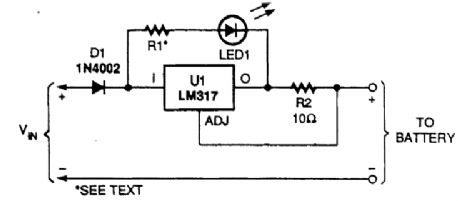
This circuit uses an LM317 as a current regulator to limit charging current to a lead-acid battery.R2 should produce a 1.2-V drop at the desired limiting value of charging current. (View)
View full Circuit Diagram | Comments | Reading(5357)
SIMPLE_LAMP_PULSER
Published:2009/6/19 2:50:00 Author:May
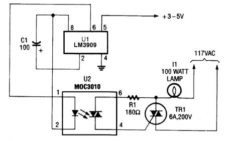
Here, the LM3090 (configured as a timing oscillator) is used to control a 117-Vac lamp through an MOC3010 optois olator/coupler. (View)
View full Circuit Diagram | Comments | Reading(2124)
SYN_COMBINER
Published:2009/6/19 2:38:00 Author:May
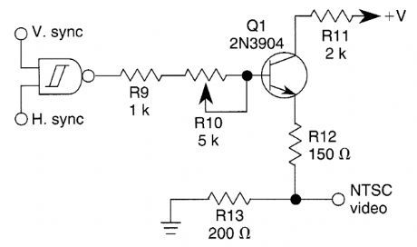
This circuit combines H and V sync signals at TTL or CMOS levels and produces an NTSC video sync output. (View)
View full Circuit Diagram | Comments | Reading(1838)
SAW_FILTER_IMPEDANCE_MATCHING
Published:2009/6/19 2:34:00 Author:May
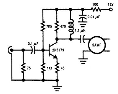
This circuit matches a saw ffiter to an IF amplifier. (View)
View full Circuit Diagram | Comments | Reading(1029)
TYPICAL_TWO_WAY_SWITCH_WIRING
Published:2009/6/19 2:23:00 Author:May
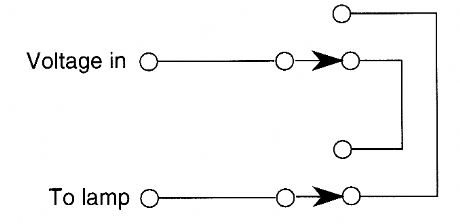
When the light is off, it can be turned on with either switch. When it's on, it can be turned off with either switch. (View)
View full Circuit Diagram | Comments | Reading(783)
CIGRETTE_LIGHTER_9_V_ADAPTER
Published:2009/6/19 2:18:00 Author:May
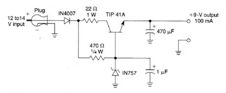
A simple way to provide +9 V at 100 mA from a 12-V auto source. Applications include small radios, cassettes, etc. (View)
View full Circuit Diagram | Comments | Reading(807)
TRANSISTOR_MATCHING_CIRCUIT
Published:2009/6/19 2:11:00 Author:May
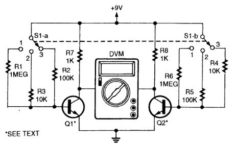
In order to match two transistors, select Q1 and Q2 so that they give zero readings(or as close as possible)on a DVM. The DVM acts as a null detector. An analog meter can be substituted. S1 should be set for an appropriate level of base current(approximately 8,80,or 800 μA). (View)
View full Circuit Diagram | Comments | Reading(1505)
REFERENCE_CIRCUIT
Published:2009/6/19 2:09:00 Author:May
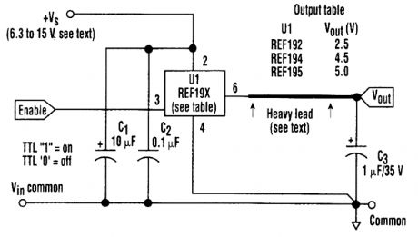
In this high-performance reference circuit, U1 is a device from the REF190 series producing de-vice-selectable outputs of 2.5, 4.5, and 5 V with simple, noncritical external circuitry. An Analog Devices REF 19 X(see the table in the figure)is used to derive a reference voltage. (View)
View full Circuit Diagram | Comments | Reading(1000)
SIMPLE_LOCK
Published:2009/6/19 1:44:00 Author:May
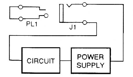
Only an appropriately wired plug of the right size will activate circuits with a nonshorting jack in their power supply circuit. (View)
View full Circuit Diagram | Comments | Reading(796)
ELECTRONIC_LOCK
Published:2009/6/19 1:36:00 Author:May
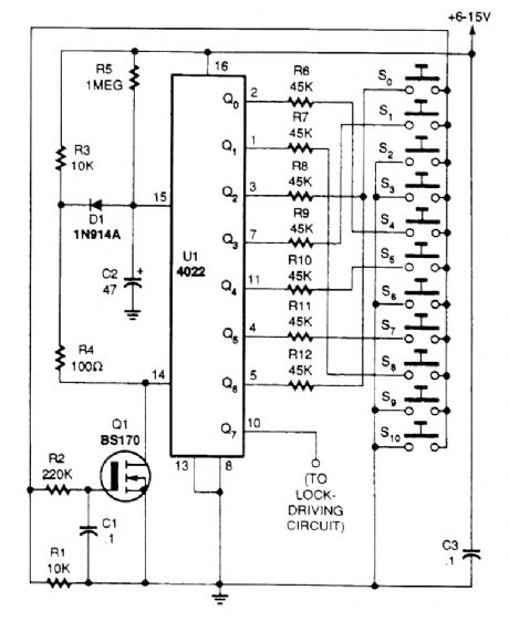
The heart of the circuit is a 4022 octal counter. When first powered up, C2 is charged via R5, so the reset input of the couitter is kept high. That causes output Qo to go high while all other outputs are low. With the switches wired as shown, when 54 is pressed, the BS170 is switched on via de-bouncing network R2/C1, and U1 receives a clock pulse. Also, C2 is discharged via R4 and D1 removing the reset signal of the counter, allowing it to advance. The time required for C2 to charge via R5 (e.g., to reset the counter), is the maximum time that can lapse before the next key is pressed.The above cycle is therefore repeated only if S8 (connected to the Q1 output) is pressed in time.When all keys have been pressed in time and in the correct order, Q7 goes high for about four sec-onds to drive the unlock circuitry (e.g., a relay driver for an automatic door opener. A builder can change the code by reviewing the switches. The code for the lock shown in the circuit diagram is 4-8-0-1-5-7-0. However, the 4022 octal counter can be replaced by a 4017 divide-by-10 counter. That will make it possible to add two more digits to the combination. (View)
View full Circuit Diagram | Comments | Reading(4)
BIPOLAR_STEPPER_MOTOR_DRIVE_CIRCUIT
Published:2009/6/18 23:39:00 Author:May
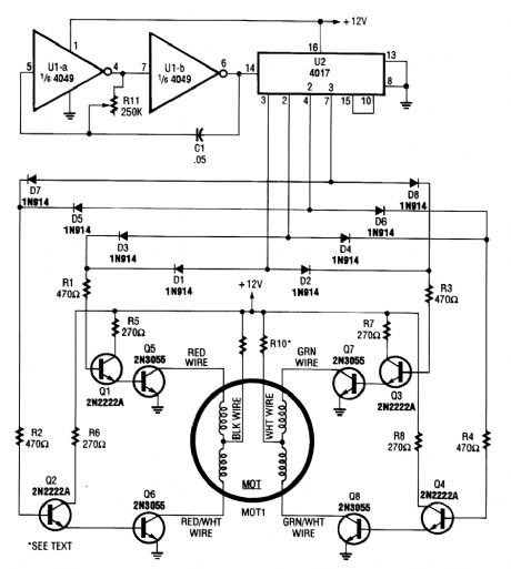
A 4017 decade counter/divider driven from a low-frequency oscillator (U1-a and U1-b) is used to drive transistor switches to sequence the windings, as is needed. MOT1 is a 12-V stepper motor. R9 and R10 are selected for the motor's current rating. A 3.3-Hz signal from UI will cause the motor to run at 1 rpm, a 33-Hz signal will result in 10 rum, etc. (View)
View full Circuit Diagram | Comments | Reading(2301)
VARIABLE_VOLTAGE_ATTENUATOR
Published:2009/6/18 23:28:00 Author:May
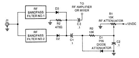
The front-end of this circuit is a bank of selectable bandpass filters. The output of the filter banks are shunted to ground via capacitor (C1) and PIN diode (D1). The PIN diode acts like an electroni-cally variable resistor. The resistance across the diode's terminals is a function of the applied bias voltage. This voltage, hence the degree of attenuation of the RE signal, is proportional to the setting of potentiometer RI. The series resistor (R2) is used to limit the current when the diode is forward biased. This step is necessary because the diode has a very low resistance when a certain rather low potential is exceeded. (View)
View full Circuit Diagram | Comments | Reading(862)
SWITCHABLE_POWER_ATTENUATOR
Published:2009/6/18 23:27:00 Author:May
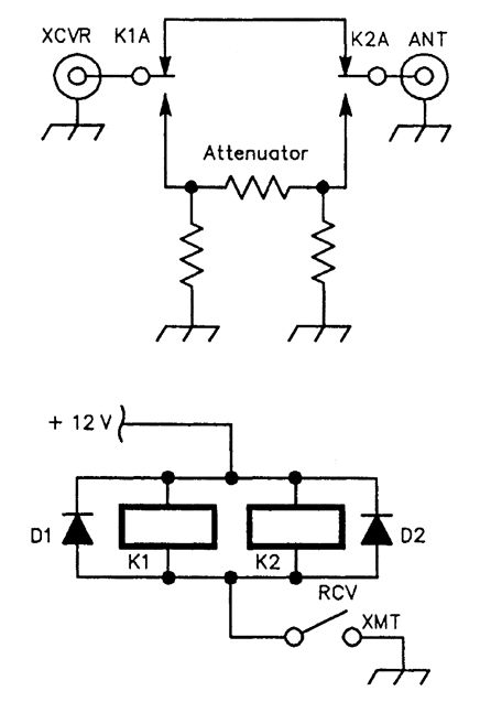
Schematic diagram of a switchable power attenuator that can be used to reduce the power output of transmitters that don't have ALC lines.
Values for 10 and 20 dB: 10 dB: R1 = R3 = 91 ΩR2 = 75 Ωnearest standard values 20 dB: R1 = R3 = 62Ω R2= 240 Ω nearest standard values
Note: R1 must handle the largest share of the input power, and R2 somewhat less. This depends on attenuation selected. (View)
View full Circuit Diagram | Comments | Reading(674)
| Pages:18/24 1234567891011121314151617181920Under 20 |
Circuit Categories
power supply circuit
Amplifier Circuit
Basic Circuit
LED and Light Circuit
Sensor Circuit
Signal Processing
Electrical Equipment Circuit
Control Circuit
Remote Control Circuit
A/D-D/A Converter Circuit
Audio Circuit
Measuring and Test Circuit
Communication Circuit
Computer-Related Circuit
555 Circuit
Automotive Circuit
Repairing Circuit