
Index 171
SHUNT_CLIPPER
Published:2009/7/13 21:14:00 Author:May
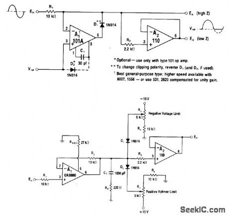
When input voltage is above reference voltage, D1 is reverse-biased and input voltage passes through R1 to output.When negative peak of Ein exceeds Vref, opamp A1 turns D1 on to absorb input current from R1, thereby clamping output at level of Vref. If low output impedance is required, use 110 highspeed voltage follower as buffer amplifier.-W.G. Jung, IC Op-Amp Cookbook, Howard W.Sams, Indianapolis, IN, 1974, p 189-190. (View)
View full Circuit Diagram | Comments | Reading(1233)
NEON_INDICATOR_SCALER
Published:2009/7/13 21:10:00 Author:May
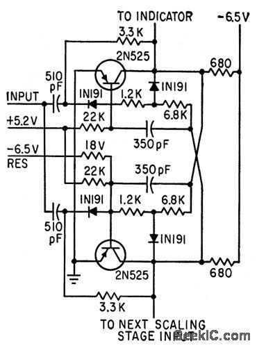


Battery-powered stage uses binary scaling circuit with nonsaturated temperature-compensated transistors, as elements of scale-of-64 circuit driving 4-dight mechanical register.-F.E. Armstrong. Battery Powered Portable Scaler.Electronics.33:19,p74-75 (View)
View full Circuit Diagram | Comments | Reading(806)
MAX038_HIGH_SPEED_FUNCTION_GENERATOR_CIRCUIT
Published:2009/7/13 21:07:00 Author:May
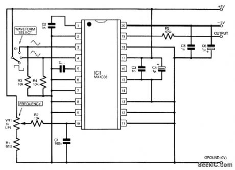
For enthusiasts who would like to experiment with this device for themselves, a simple circuit to get it up and running is shown. The only real problem with the MAX038 is inherent in its sheer speed. Maxim suggests careful layout on adouble-sided ground-plane PC board for best results. In practice, a single-sided PC board seems to work well, provided it has plenty of copper areas at ground potential, good decoupling, and guard tracks around signal paths carrying rectangularwaveforms, especially that from the sync output. The following component recommendations are offered:Resistors-0.6 W, 1-percent metal filmC1, C2, C3, and C5-ceramic diskC4 and C6-tantalum bead, 35 VCext-as required for frequency, between 47pF and 47μF, polyester or polystyrene (View)
View full Circuit Diagram | Comments | Reading(1594)
VLF_CONVERTER
Published:2009/7/13 21:05:00 Author:May

This very simple converter permits reception of the VLF 3- to 30-kHz band on a shortwave receiver covering the 6-MHz (49-m) shortwave broadcast band. T1 is an audio transformer of about 8 to 1000ΩThese can easily be purchased new or found in junked transistor radios. (View)
View full Circuit Diagram | Comments | Reading(0)
GUNSHOT_COUNTER
Published:2009/7/13 20:57:00 Author:May
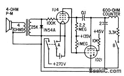
Loudspeaker serves as microphone for picking up loud noises such as from blasts, noisy auto engines, and children on roller skates. Each input shock wave drives grid of 1U4 negative and fires 1D21 strobotron, thereby dumping charge on 2.mfd capacitor from plate to ground through counter. Operates at up to 40 shots per second, fast enough for most automatic weapons fire.-R. L. lves , Shot Counter Uses Strobotron, Electronics, 31:33, p94-96. (View)
View full Circuit Diagram | Comments | Reading(887)
COLD_CATHODE_FLUORESCENT_LAMP_DRIVER
Published:2009/7/13 20:55:00 Author:May
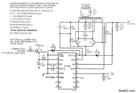
In this circuit, the lamp is driven sinusoidally, minimizing RF emissions in sensitive portable applications. Lamp intensity is controlled smoothly from zero to full brightness with no hysteresis or pop on. This floating bulb circuit configuration extends the illumination range for the bulb because parasitic bulb-to-display-frame capacitive losses are minimized. The feedback signal is generated by monitoring the primary-side Royer converter current between the BAT and Royer pins. The LT1184F current-mode switching regulator and L2 provide an average current to Q1 and Q2, which form a Royer-class converter along with L1 and C1. The lamp is driven by L1's secondary. Feedback to the LT1184F is provided on the primary side of L1 for floating bulb configurations, whereas feedback in the grounded configuration is provided by sensing one-half of the average bulb current. The oscillator frequency is 200 kHz, which minimizes the size of the required magnetics.
(View)
View full Circuit Diagram | Comments | Reading(1837)
ENHANCED_TUNNEL_DIODE_NOR_CIRCUIT
Published:2009/7/16 1:54:00 Author:Jessie
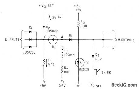
Clock pulse through D2 triggers tunnel diode to its high voltage state to produce an output only when there are no inputs. Hybrid circuit will operate above 100 Mc, ct high fan-in and fan-out, and uses low-cost parts.-P. Chow and J. Cubert, A Key to Nanosecond Switching, Electronics, 36:42, p 42-45. (View)
View full Circuit Diagram | Comments | Reading(817)
TUNNEL_DIODE_THIN_FILM_TOGGLING_CIR_CUIT
Published:2009/7/16 1:53:00 Author:Jessie
Supply biases flim-diode combination at constant 5 v at 25 ma so two stable diode voltages are about 0.05 and 0.4 v. This means that bias current through film winding will flow in either of two directions, depending on state of diode.-T. A. Smay and A. V.Pohm, Design of Logic Circuits Using Thin Films and Tunnel Diodes, Electronics, 34:35, p 59-61. (View)
View full Circuit Diagram | Comments | Reading(606)
OPTOISOLATOR_DRIVE_FOR_240_VAC_LOAD
Published:2009/7/13 20:50:00 Author:May
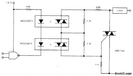
wo Motorola M0C3011 optically coupled triac drivers are used in series to overcome voltage limhation of single coupler when triggering triac connected to control 240-VAC load. Two 1-megohm resistors equalize voltage drops across couplers.-P.O'Neil, Applications of the MOC3011 Triac Driver, Motorola, Phoenix,AZ,1978,AN-780,p5. (View)
View full Circuit Diagram | Comments | Reading(1096)
SENSE_AMPIJFIER
Published:2009/7/16 1:52:00 Author:Jessie
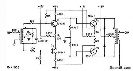
Minimum input required from cores of random-access memory is 30 mv, and minimum output pulse is 6 v. Amp lifier is balanced to reduce common-modenoise.-G. E. Lund and D. R. Faulis, Expandable Random Access Memories, Electronics, 33:11, p 164-166. (View)
View full Circuit Diagram | Comments | Reading(629)
TRIAC_FOR_INDUCTIVE_LOADS
Published:2009/7/13 20:48:00 Author:May
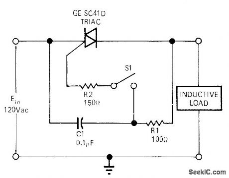
Simple triac gating circuit applies AC power to inductive load when low-power switch S1 is closed. R1 and C1 provide dv/dt suppression.-C. A. Farel and D. M. Fickle, Triac Gating Circuit, EDN/EEE Magazine, Jan. 1, 1972, p 72-73. (View)
View full Circuit Diagram | Comments | Reading(2716)
DIODE_GATE
Published:2009/7/16 1:52:00 Author:Jessie
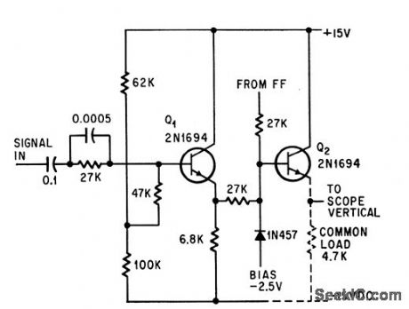


Input signal from ring counter applies reverse bias through isolating transistor Q1 to diode gate and base of Q2, which then supplies current to common load of multichannel scope display.-J. E. Russell, Ten Signals at a Glance, Electronics, 37:19, p 54. (View)
View full Circuit Diagram | Comments | Reading(779)
400_Hz_TRIGGER_FOR_SCR
Published:2009/7/13 20:44:00 Author:May
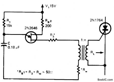
Simple UJT oscillator combined with pulse transformer provides pulses required for firing 2N1764 SCR.Article gives design data for pulse transformer,along with design equations.-W. Dull, A, Kusko, and T. Knutrud, Pulse and Trigger Transformers-Performance Dictates Their Specs, EDN Magazine, Aug. 20, 1976, p 57-62. (View)
View full Circuit Diagram | Comments | Reading(1145)
DIGIT_LINE_DECOUPLER
Published:2009/7/16 1:51:00 Author:Jessie
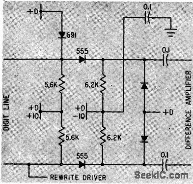
Diode switch and biasing network disconnect sense amplifier, allowing common-mode signal of about 1 v to reach difference amplifier. This signal is almost completely rejected at output, so amplifier is ready for next cycle 0.5 microsec after end of rewriting.-A. Melmed, R. Shevlin, and W. Orvedahl, Diode Steering Increases Speed of Magnetic Memories, Electronics, 34:37, p 68-70. (View)
View full Circuit Diagram | Comments | Reading(650)
SIGNAL_BRIDGE_FET
Published:2009/7/16 1:51:00 Author:Jessie


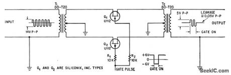
Provides pulsed c-w output from 300- kc c-w input.On-off ratio is 50 db. Insertion loss is 15 db with 510-ohm output load. Requires no adjustment. Used in sonar experiments.-F. J. Murphree and J. Bealor, FET in Bridge Circuit Gates a 300-KC Signal, Electronics, 38:9, p 60-61. (View)
View full Circuit Diagram | Comments | Reading(645)
NEON_TRIODE_OFF_ON_GATE
Published:2009/7/16 1:50:00 Author:Jessie
Supply voltage is set midway between firing and extinction voltages of neon tube. Neon conducts when triggered by momentary increase in voltage, and continues conducting until supply voltage is momentarily lowered below extinction voltage. Can be used to produce Low-repetition-rote pulses. Triode may be 6AV6 or 1/2 12AXT.-R. L. Lves, Neon Triode Gives Low- Speed Gate, Electronics, 31:11, p 170-174. (View)
View full Circuit Diagram | Comments | Reading(632)
BUTTON_AND_BEAD_COUNTER
Published:2009/7/13 20:36:00 Author:May
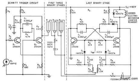
Tiny objects passing before photodiode are counted by Schmitt trigger and four binary stages at up to 30 counts per second, with electromechanical counter readout.-E. J. Brach, Photocell Triggers Counting Circuit, Electronics,38:13,p74-75 (View)
View full Circuit Diagram | Comments | Reading(752)
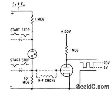
27_MC_RECEIVER_FOR_TONE_MODULATED_DATA
Published:2009/7/13 20:35:00 Author:May
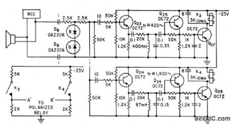
Two selective amplifiers, one tuned to 400 cps and other to 1,400 cps, drive relays K3 and K4 to control printing register for recording remote events such as passage of birds through infrared curtain.-P. A. love and J. Czekajewski, Infrared Curtain System Detects and Counts Moving Objects, Electron-ics, 34:31, p40-43. (View)
View full Circuit Diagram | Comments | Reading(632)
28_TO_420_V_D_C_CONVERTER
Published:2009/7/13 20:27:00 Author:May
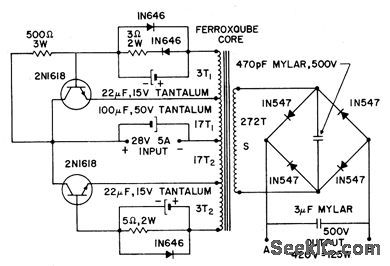
Efficiency is 87%, power output 125w, output voltage ripple 0.7V p-p, and operating frequency 10 kc. Ambient temperature range is -50 to 125℃. Transformer winding data is given.- Transistor Manual, Seventh Edition, General Electric Co.1964, p238. (View)
View full Circuit Diagram | Comments | Reading(643)
ELECTROLUMINESCENT_PANEL_DRIVER
Published:2009/7/13 20:27:00 Author:May
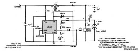
Driving electroluminescent (EL) panels, such as those used for backlighting LCD screens in portable devices,is a challenge because they are capacitive loads and require high-voltage ac drive signals. Typically, EL panels exhibit about 3 nF/in2 capacitance. The LT1305 circuit shown can drive an EL panel with up to 100 nF total capacitance. The LT1305 micro power dc-to-dc converter contains an internal power switch capable of up to 2 A switch current. The high-power switch drives the primary of fly back transformer T1. A minimum input voltage of 1.8 V ensures operation with two-cell supplies. The input voltage is boosted to a voltage that ranges from 166 to 248 Vdc, as set by R1. The ac drive waveform is created by an external square-wave control signal turning on and off the NPN transistor, bringing point A to ground and inverting the voltage across the panel and then returning to a high positive voltage. By adjusting R1, the panel ac drive voltage can be set from 83 to 115 Vrms to alter the display brightness. The color or hue of the display can also be slightly varied by changing the frequency of the square-wave drive signal. This control signal can be from a system microprocessor output pin. (View)
View full Circuit Diagram | Comments | Reading(2531)
| Pages:171/471 At 20161162163164165166167168169170171172173174175176177178179180Under 20 |
Circuit Categories
power supply circuit
Amplifier Circuit
Basic Circuit
LED and Light Circuit
Sensor Circuit
Signal Processing
Electrical Equipment Circuit
Control Circuit
Remote Control Circuit
A/D-D/A Converter Circuit
Audio Circuit
Measuring and Test Circuit
Communication Circuit
Computer-Related Circuit
555 Circuit
Automotive Circuit
Repairing Circuit