
Index 175
D_C_TO_D_C_VOLTAGE_BOOSTER
Published:2009/7/13 5:46:00 Author:May
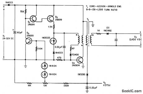
Depends on alternate storing and retrieving of energy from magnetic field of ringing choke. Uses blocking oscillator Q1 to chop input signal.Darlington pair Q1-Q2 provides high input impedance. Q3 is regulating transistor, and Q4 is blocking oscillator. Provides isolated 2,400 v output and 375V output.-J. F.Howell, Ringing Choke Simplifies D-C to D-C Conversion, Electronics, 39:8, p90-92. (View)
View full Circuit Diagram | Comments | Reading(1071)
ANALOG_FLUXGATE_MAGNETOMETER_ASSEMBLY
Published:2009/7/13 5:45:00 Author:May
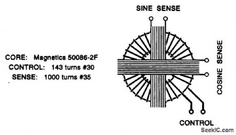
An audio input drives the sine-wave control input, switching (or gating ) the core in and out of saturation and drawing in or releasing an external magnetic field.Weak signals at the sense outputs are proportional to field strength. (View)
View full Circuit Diagram | Comments | Reading(1403)
VOLTAGE_FREQUENCY_CONVERTER
Published:2009/7/13 5:40:00 Author:May
Linear voltage-controlled variable-frequency oscillator converts standard recorder to low.frequency f-m recorder for 0.1 to 1,000-cps signals. Values are: R1-18,000; R2-100,000; C-0.01 mfd; R-10,000; Q1-2N591; Q2-2N491; Vcc-20v; R4-270; fo-2.5 kc.-J.Schwartz, Unijunction Transistor Simplifies Voltage-Frequency Converter, Electronics, 36:43, p56. (View)
View full Circuit Diagram | Comments | Reading(1681)
RINGING_CHOKE_CONVERTER_REGULATOR
Published:2009/7/13 5:34:00 Author:May
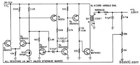
Steps up 32-V d-c pulses to 2.500-V d-c pulses,with regulation of 0.02%, achieved by sampling output and feeding it back to comparision circuit. Uses unijunction transistor Q3 with 04 for pulse generation.-J. F. Howell,Ringing Choke Simplifies D-C to D-C Conversion, Electronics, 39:8, p90-92. (View)
View full Circuit Diagram | Comments | Reading(2222)
AUTO_SIGNAL_MINDER
Published:2009/7/13 5:30:00 Author:May
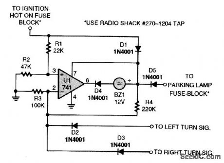
If the ignition is on and the parking lights are on or off, the noninverting input of U1 is at 8 V and the inverting input is either 0 or 4 V. That causes pin 6 to go high, keeping the buzzer off. If the ignition is off and the parking lights are on, the noninverting input is at 0 V and the inverting input is at 4 V. That brings pin 6 low, activating the buzzer. With the ignition and turn signal on and the parking lights on or off, the noninverting input is at 8 V and the inverting input pulses at 12 V, causing the buzzer to sound in step with the blinker. (View)
View full Circuit Diagram | Comments | Reading(939)
NEGATIVE_IMPEDANCE_CONVERTER
Published:2009/7/13 5:28:00 Author:May
Increases circuit Q by factor of 4 or more in tuned audio circuits by reducing circuit losses.-W. P, Delaney, New Way to Multiply Q with Transistors, Electronics, 35:28, p48-49. (View)
View full Circuit Diagram | Comments | Reading(1043)
AUTOMATIC_VEHICLE_DOOR_UNLOCK_CIRCUIT
Published:2009/7/13 5:26:00 Author:May
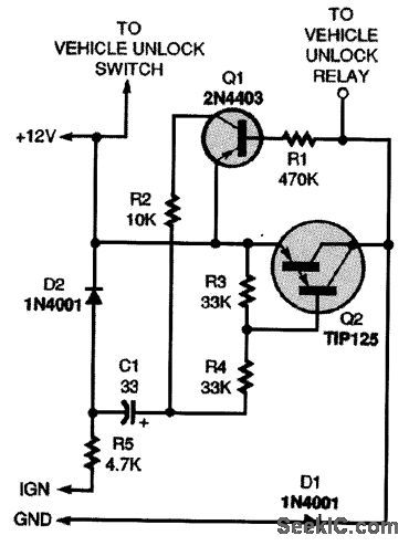
When the ignition switch is on, the +12V and IGN lines connected to the circuit are within half a volt or so of each other. Resistor R3 reverse-biases Darlington Q2 and keeps it cut off. Transistor Q1 is in parallel with Q2's emitter and collector; Q1 is ON as a result of the large voltage drop across Q2's emitter and collector. When the ignition switch is turned off, voltage is removed from the IGN line, effectively placing R5 at ground level. Capacitor C1 provides a path for current to flow through R3 to R5 and the vehicle components to ground. That flow will forward-bias Q2, driving it into saturation and lowering its emitter/collector voltage to less than 0.5 V. As a result, almost full battery voltage is applied to the vehicle unlock relay; transistor Q1 is cut off at the same time. The voltage divider of R3 and R4 prevents false triggering during voltage sags on the IGN line. (View)
View full Circuit Diagram | Comments | Reading(964)
SW_CONVERTER
Published:2009/7/13 5:24:00 Author:May
This simple circuit, built around a NE602, allows you to receive either the 6- or 9.5-MHz shortwave band on your car radio. (View)
View full Circuit Diagram | Comments | Reading(969)
END_OF_TRANSMISSION_BEEPER
Published:2009/7/13 5:21:00 Author:May
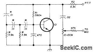
Release of push-to-talk (PTT) switch at end of radio conversation activates time delay for antenna changeover relay, keeping transmitter on air long enough to transmit 800-Hz tone burst indicating transmission termination. Tone is generated in simple one-transistor phase-shift oscillator powered by voltage present between PTT terminal and ground in receive mode of transceiver, which may be any voltage between 6 and 30 VDC. Transistor can be any small-signal NPN silicon with gain of at least 300 at 1 mA, such as 2N930. Parts marked with asterisk must be matched within 5%.-E. Hombostel, Automatic Beeper for Station Control, Ham Radio, Sept. 1976, p 38-39. (View)
View full Circuit Diagram | Comments | Reading(1070)
FISH_SHOCKER
Published:2009/7/16 2:40:00 Author:Jessie
Two thyratrons serve as d-c interrupter that alternately connects and disconnects d-c generator from load consisting of fresh-water path between aluminum boat and aluminum grid 6 ft away. Fish swim toward positive electrode, receive shock, and are temporarily stunned. Timing circuits de. termines number and duration of pulses.-H. P. Dale, Electronic Fishing with Underwater Pulses, Electronics, 32:4, p 31-33. (View)
View full Circuit Diagram | Comments | Reading(7133)
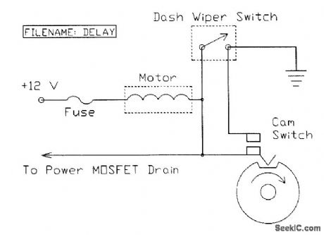
WINDSHIELD_WIPER_CIRCUIT
Published:2009/7/13 5:19:00 Author:May

When the wipers are turned on, the switch in parallel with the cam-operated points keeps the motor running. When the switch is tumed off, the motor keeps running until the cam opens the points, stopping the motor when the wipers are in the PARK position. (View)
View full Circuit Diagram | Comments | Reading(964)
MATCHING_LOW_Z_MIKE
Published:2009/7/13 5:18:00 Author:May
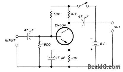
Single-transistor microphone impedance-matching circuit for low-impedance microphone feeds high-impedance input of amateur SSB transceiver. Circuit also boosts gain enough to meet transmitter input requirements.-C. Drumeller, Active Microphone Impedance Match, Ham Radio, Sept. 1973, p 67-68. (View)
View full Circuit Diagram | Comments | Reading(2900)
FAST_CLAMP
Published:2009/7/13 5:16:00 Author:May
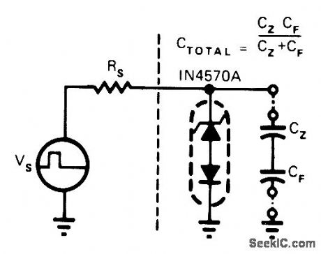
Smaller capacitance of temperature-compensated reference diodes allows clamping of faster pulses than is possible with ordinary zeners. Diagram shows positive 6.4-V diode clamp at ground potential. For smaller zener voltages, connect diode to more negative potential. Device Iimits only positive peaks; for negative peaks, reverse connections to 1N4570A. To clamp both polarities, use two units in parallel, oppositely connected.-W.Walloch, Clamp Fast Pulses with one Component, EDN Magazine, AprilG, 1974, p 76. (View)
View full Circuit Diagram | Comments | Reading(882)
CAPACITOR_DISCHARGE_IGNITION_CIRCUIT
Published:2009/7/13 5:15:00 Author:May
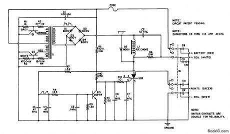
This ignition circuit consists of a dc-to-dc converter delivering 250 to 300 V to a 1.5-mF capacitor, and discharging it through the ignition coil primary upon the opening of the distributor points. SCR is triggered by the opening of the distributor points via inverter and pulse shaper Q3 and associated components. This circuit is typical of CD ignition systems. T1 is a special transformer for this circuit, but any suitable dc-to-dc converter transformer and circuit that delivers 250 Vdc (or more) can be used. (View)
View full Circuit Diagram | Comments | Reading(4394)
CLIPPER_STROBE
Published:2009/7/13 5:14:00 Author:May
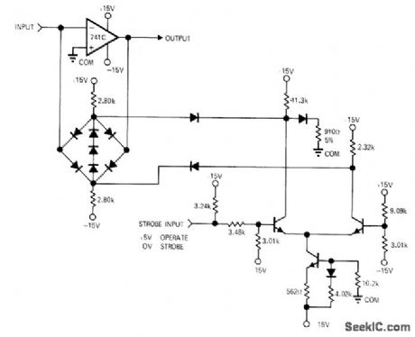
Combination strobe and clipper built around 741C opamp provides two basic functions. First, strobe input of 5 V can reduce gain of amplifier to nearly zero by shorting output to input. Second, clipping function holds all outputs below predetermined level. When used in integrator, circuit provides constant rate of discharge for integrating capacitor. Clipping is done by four-diode bridge having three extra diodes acting as zener. Strobe function is provided by four-diode bridge alone, with strobing input circuit having single-ended input and differential output All transistors are 2N2219,and all diodes are 1N914.-L .Strahan,op Amρ Control Without Reays,EDN /EEE Magazine,Aug,15,1971,p 41-42.
(View)
View full Circuit Diagram | Comments | Reading(710)
VOICE_OPERATED_GATE
Published:2009/7/13 5:13:00 Author:May
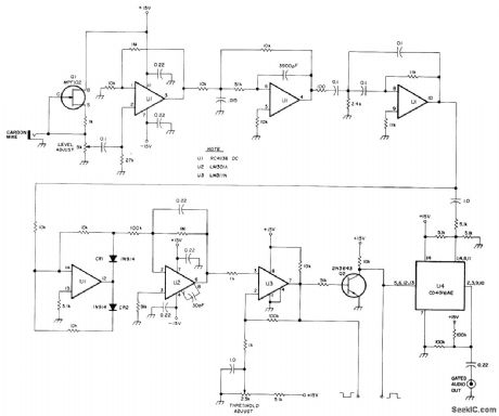
Uses four ICs, two transistors, and two diodes to accomplish preamplification, bandpass filtering, and audio gating, as replacement for voice-operated relay in SSB transceiver having carbon microphone, Logic output (with choice of 1 or 0) serves as turn-on signal for other sections of system being voice-controlled. Low-pass and high-pass active filter pair provides equivalent of 300-3000 Hz bandpass filter with 40 dB rolloff per decade at each edge, to discriminate against ambient noise. Q1 is FET constant-current source for carbon microphone, feeding preamp U1 that provides voltage gain of about 100 and output of about 3 VRMS. Next two sections of quad opamp U1 are active filters, and last section of U1 is active diode detector in which opamp linearizes detector CR1-CR2. Rectified audio is averaged by U2 to give smoothed long positive pulse with duration of audio burst.Schmitt trigger U3 sharpens pulse and makes it compatible with CMOS logic. Inverter Q2 turns on analog gate U4 when audio signal is present.-H. Olson, Voice-Operated Gate to Replace Voice-Operated Relays for Carbon Microphones, Ham Radio, Dec. 1977, p 35-37. (View)
View full Circuit Diagram | Comments | Reading(1312)
MICROPOWER_FIELD_DETECTOR_FOR_470_MHz
Published:2009/7/13 5:10:00 Author:May
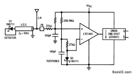
This circuit, which was tested at 470 MHz, contains a couple of improvements over the standard L/C-with-whip field-strength meter. The 0.4-wavelength section presents an efficient, low-impedance match to the base of the quarter-wave whip, but transforms the received energy to a relatively high voltage at the diode for good sensitivity. Biasing the detector diode improves the sensitivity by an additional 10 dB. The detector diode's bias point is monitored by an LTC1440 ultra-low-power comparator and by a second diode, which serves as a reference. Schottky diode D1 rectifies the incoming carrier and creates a negative-going bias shift at the noninverting input of the comparator. Note that the bias shift is sensed at the base of the antenna, where the impedance is low, rather than at the Schottky, where the impedance is high. This introduces less disturbance into the tuned antenna and transmission-line system. The falling edge of the comparator triggers a one-shot, which temporarily enables answer-back and other pulsed functions. Total current consumption is approximately 5 μA. Alternatively, a discrete one-shot constructed from a quad NAND gate draws negligible power. Sensitivity is excellent. The finished circuit can detect 200 mW radiated from a reference dipole at 100 ft. Range, of course, depends on operating frequency, antenna orientation, and surrounding obstacles; in the clear, a more reasonable distance, such as 10 ft, can be covered at 470 MHz with only a few milliwatts. All selectivity is provided by the antenna itself. Add a quarter-wave stub (shorted with a capacitor) to the base of the antenna for better selectivity and improved rejection of low-frequencysignals. (View)
View full Circuit Diagram | Comments | Reading(874)
AUTOMOTIVE_NEON_DRIVER
Published:2009/7/13 5:09:00 Author:May
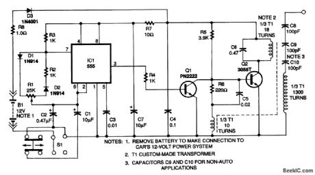
A 555 timer drives driver transistor Q1 and switching transistor Q2 at 25 to 30 kHz. T1 is wound on a ferrite core (try using a core from an old B/W TV flyback) and has the windings arranged as shown in the schematic. About 2500 Vac p-p is produced, so be careful to avoid any possibility of contact with this voltage, as it can cause a bad shock or RE burn. The neon tube is a custom-size item that can be made up at any neon sign shop or possibly purchased commercially. It is not legal to illuminate certain parts of your vehicle in some parts of the United States and in some nations. (View)
View full Circuit Diagram | Comments | Reading(2042)
RADIO_AUTOMATIC_LEVEL_CONTROL
Published:2009/7/13 5:06:00 Author:May
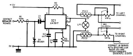
This experimental circuit automatically increases the volume of a car radio when the vehicle's speed (and consequently road and wind noise) rises, and retums the volume to a pleasant level at lower speeds. This relieves the driver of the distracting chore of continually fiddling with the radio's volume control. In the figure, a special tachometer IC type LM2917 takes its input from the ignition system's contact bre.aker points and converts this into a voltage that is directly proportional to engine speed. This voltage will always be in the range of 0 to 5 V anct is used to illuminate a miniature filament lamp LP1. On either side of this lamp is mounted a pair of light-dependent resistors (LDRs) that are connected in series with the wipers of the radio's volume control potentiometers. A ganged potentiometer across each of the LDRs sets the minimum volume level, the radio's own volume being used for the high level. The value of capacitor C2 determines the range over which the unit will function satisfactorily. A suggested value of 4n 7 would be a suitable starting point for further experimentation. The 100-kΩ input resistor (R1) should be placed as near as possible to the ignition coil to prevent RFI (radio frequency interference) and to ensure that the contact breakers are not shorted out should the wire short to earth (chassis) for any reason. (View)
View full Circuit Diagram | Comments | Reading(896)
LOGIC_DRIVE_FOR_INDUCTIVE_LOAD
Published:2009/7/13 5:04:00 Author:May
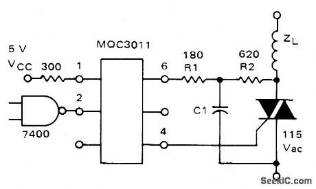
When output of NAND gate goes high and furnishes 10 mA to LED of Motorola M0C3011 optically coupled triac driver, output of optoisolator provides necessary trigger for triac controlling inductive load.C1 is 0.22 μF for load power factor of 0.75 and 0.33 μF for 0.5 power factor. Omit C1 for resistive load. R1, R2, and C1 serve as snubber that limits rate of rise in voltage applied to triac.-P. O'Neil, Applications of the MOC3011 Triac Driver, Motorola, Phoenix, AZ, 1978, AN-780 p 2. (View)
View full Circuit Diagram | Comments | Reading(1247)
| Pages:175/471 At 20161162163164165166167168169170171172173174175176177178179180Under 20 |
Circuit Categories
power supply circuit
Amplifier Circuit
Basic Circuit
LED and Light Circuit
Sensor Circuit
Signal Processing
Electrical Equipment Circuit
Control Circuit
Remote Control Circuit
A/D-D/A Converter Circuit
Audio Circuit
Measuring and Test Circuit
Communication Circuit
Computer-Related Circuit
555 Circuit
Automotive Circuit
Repairing Circuit