
Index 167
SEISMIC_RADIO_BEACON_GEOPHONE_AMPLIFIER
Published:2009/7/13 22:23:00 Author:May


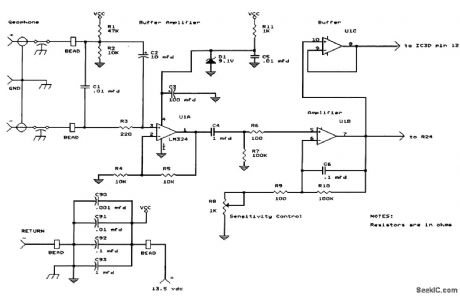
This geophone amplifier and buffer was used as part of an amateur radio beacon that monitors seismic activity in an earthquake-prone area of the United States.
(View)
View full Circuit Diagram | Comments | Reading(2968)
80_dBV_INPUT_RANGE
Published:2009/7/13 22:18:00 Author:May
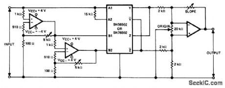
Logamp using Texas Instruments SN56502 or SN76502 in combination with three SN52741 opamps can handle input voltage range greater than 80 dB with respect to 1 V P-P. Inputs are limited by reducing supply voltages of input amplifiers to 14 V.Gains of input amplifiers are adjusted to achieve smooth transitions.- The Linear and Interface Circuits Data Bookfor Design Engineers, Texas Instruments, Dallas, TX, 1973, p 7-45. (View)
View full Circuit Diagram | Comments | Reading(815)
600_W_TRIGGERED_SCR
Published:2009/7/13 22:15:00 Author:May
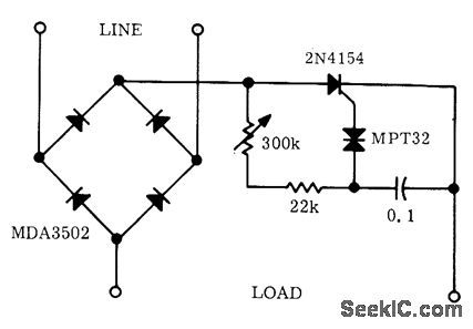
2N4154 SCR is operated from DC output of bridge rectifier and triggered by MPT32 at setting determined by position of 300K pot. Circuit provides full-wave DC control of lamp and other loads up to 600 W, using relaxation oscillator operating from DC source.- SCR Power Control Fundamentals, Motorola, Phoenix, AZ, 1971, AN-240, p 6. (View)
View full Circuit Diagram | Comments | Reading(1088)
LINE_VOLTAGE_COMPENSATION
Published:2009/7/13 22:05:00 Author:May
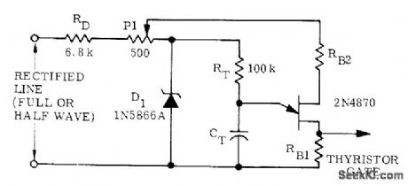
Can be used with either half-wave or full-wave phase control circuit to make load voltage independent of changes in AC line voltage.P1 is adjusted to provide reasonably constant output over desired range of line voltage. As line voltage increases, P1 wiper voltage increases. This has effect of charging CT to higher voltage so more time is taken to tagger UJT. Additional delay reduces thyristor conduction angle and thereby maintains desired average voltage.-D.A. Zinder, Unijunction Trigger Circuits for Gated Thyristors, Motorola, Phoenix, AZ, 1974, AN-413, p 4. (View)
View full Circuit Diagram | Comments | Reading(832)
SELF_BUFFERED_SERIES_CLIPPER
Published:2009/7/13 22:04:00 Author:May
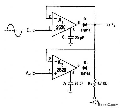
Provides negative clipping of sine.wave input, using 2620 opamps with diodes as linear OR gate. When input voltage is greater than reference voltage, A1-D1 turns on and input voltage appears at output. When Ein falls below Vref, A2-D2 provide Vref as output signal. With 2620, circuit gives good performance to above 10 kHz. For positive clipping, reverse diode connections and return R1 to +15 V. Circuit provides low output impedance.-W. G, Jung, IC Op-Amp Cookbook, Howard W. Sams, Indianapolis, IN, 1974, p 187-189. (View)
View full Circuit Diagram | Comments | Reading(797)
10_CHANNEL_MULTIPLEXER
Published:2009/7/13 22:02:00 Author:May
Basic counter consists of ten modified bistable mvbr stages, Q1 through Q20, coupled in usual ring manner and driven continuously by timing oscillator Q31. Used for multiplexing conventional or random pulse inputs from Explorer VII satellite. Eight channels serve for information inputs, and fixed levels of 0 and 110% are applied to other two channels for frame identification.-O. B. King, Multiplexing Techniques for Satellite Applications, Electronics, 32:44, p 58-62. (View)
View full Circuit Diagram | Comments | Reading(804)
LOW_VOLTAGE_BATTERY_SWITCHOVER_SYSTEM
Published:2009/7/13 22:00:00 Author:May
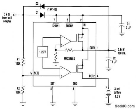
Portable systems often include the flexibility to operate either from an internal battery or from an ac-dc wall adapter. Many such systems include circuitry that switches automatically between an internal battery and an external source as the user connects and disconnects the wall adapter. The circuit shown implements this idea with a dual linear regulator, one side of which is preset for a regulated output of 2.84 V.(other versions of the IC offer 2.80-V and 3.15-V outputs). The other side of the regulator id configured to allow user-adjustable outputs, but, in this case, it monitors the wall-adapter voltage. When that voltage is removed by unplugging the adapter, the regulator's pass transistor routes battery current into the IC for support of the 2.84-V output (current flow in this transistor is counter to that of most applications). The input bypass capacitor (C1) provides enough holdup time for seamless transitions between the battery and adapter voltages. Resistors RI and R2 sense the wall-adapter voltage and determine the switchover threshold, 'VSW VSW = Vset【(R1+R2)/R2】 = 1.25V【(130kΩ+100kΩ)/100kΩ】 = 2.875vDiode Dl isolates the wall-adapter voltage so that the battery can't cause limit cycling by retriggering the switchover. D2 holds the IC's dual-mode input in the external feedback mode by maintaining a minimum voltage at the SET2 input. The wall-adapter voltage should be equal to or greater than the maximum battery voltage. (View)
View full Circuit Diagram | Comments | Reading(851)
SYMMETRICAL_BIOPLAR
Published:2009/7/13 21:59:00 Author:May
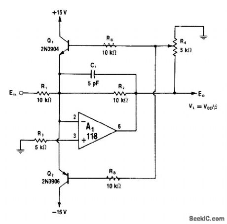
Circuit uses transistor feedback, with cument returned to opamp summing point through emitter-followers Q1 and Q2. When output E0 rises to positive voltage high enough so tap on R4, makes Q1 turn on, output of A1 is limited to value corresponding to setting of R4. Q2 performs similar limiting function for negative swings of input signal. R4 sets limiting level for both polarities, for variable symmetrical limiting. Transistors and opamps shown are selected for high-speed operation.For single-polarity limiting, insert large resistance RB in base lead of remaining transistor to prevent it from conducting heavily on output voltage swings.-W. G. Jung, IC Op-Amp Cookbook, Howard W. Sams, Indianapolis, IN, 1974, p 203-204.
(View)
View full Circuit Diagram | Comments | Reading(743)
FAST_SWITCHING_TTL_INTERFACE_FOR_VMOS
Published:2009/7/13 21:59:00 Author:May
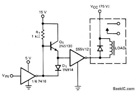
Totem-pole TTL interface drive for S55V01 VMOS gives appreciably faster switching times (less than 30 ns). To achieve fast turn-on time without unduly small pull-up resistor, which dissipates considerable power when switch is in OFF state, emitter-follower Q1 drives high peak currents into capacitive VMOS input.-L. Shaeffet, VMOS Peripheral Drivers Solve High Power Load Interface Problems, Computer Design, Dec. 1977, p 90, 94, and 96-98. (View)
View full Circuit Diagram | Comments | Reading(926)
ROCKET_LAUNCHER_VOICE_COUNTDOWN_RECORDER_CIRCUIT
Published:2009/7/13 21:57:00 Author:May
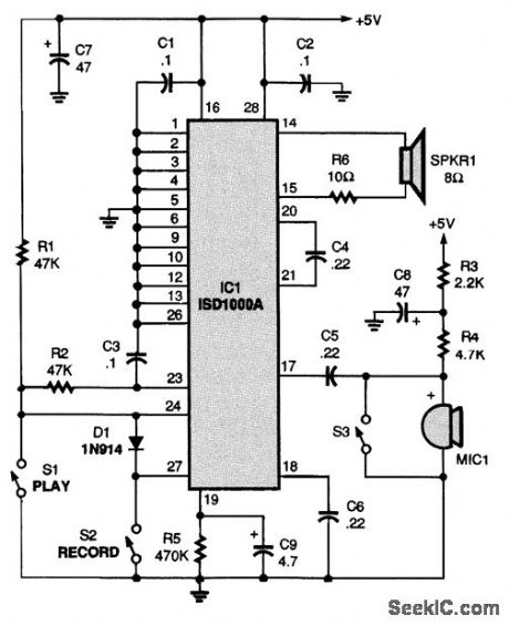
Use this circuit to record your countdown sequence on the ISD1000A. Once you are satisfied with your recording, the circuit will no longer be needed.This circuit can be used as a stand-alone voice recorder circuit. (View)
View full Circuit Diagram | Comments | Reading(4625)
SWITCHING_4500_W_AT_UP_TO_10_kHz
Published:2009/7/13 21:56:00 Author:May
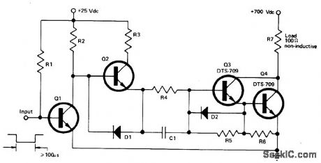
Darlington connection of Delco DTS-709 transistors will switch 7 A at 700 V with 1-μs switching time. Suitable for motor speed control,switching regulator、and inverter applications. Can be operated directly from 440-VAC line. Q1 and Q2 are 2N6100. Diodes are 1N4001 C1 is 4 μF at 15V. R1 is 510 ohms,R2 is 100, R3 is 12,R4 is l0, R5 is 1K, R6 is 47 and R7 is 100,- Low Cost'Duolithic Darlington'Switches 4500 Watts at up to 10 kHz, Delco, Kokomo,IN,1973, Application Note 54,p 2. (View)
View full Circuit Diagram | Comments | Reading(928)
HIGH_SPEED_BUFFERED_FLIP_FLOP
Published:2009/7/13 21:56:00 Author:May


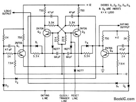
Buffering increases load-handling capacity and insures accurate counting of 10-Mc clock frequencies.-D. L. Nepveux , Digital Circuits Achieve Automatic Control of Radar Range Tracking, Electronics, 34:52, p 46-50. (View)
View full Circuit Diagram | Comments | Reading(676)
_LED_ROCKET_COUNTDOWN_LAUNCHER
Published:2009/7/13 21:53:00 Author:May
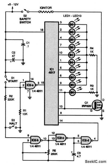
A 4011 quad two-input NAND gale and a 4017 decade-counter/divider IC are the heart of the launcher Transistor Q1,an IRF520 hexFET,sends the current through the igniter fuse to fire the rocket engine Two gates of a 4011 NAND gate,IC2-b and IC2-c,are connected in a low-frequencyoscillator circuit,with R5 and C3 setting the oscillator's frequency.Another gate of that IC,IC2-a,starts the countdown and sets pin 15 of the 4017 to the Run condition The IC's fourth gate,IC2-d,inverts and buffers the oscillator's output and supplies the clock input to pin 14 of the 4017. The 10 LEDs indicate the count. When the last one (LEDl) turns on, pin 11 goes high, turning Q1 on and firing the igniter fuse. The last LED, LED1, will remain on until S1 is switched off. The countdown can be halted by closing S3. Opening S3 continues the countdown. (View)
View full Circuit Diagram | Comments | Reading(1511)
LIMITING_PREAMP_FOR_FM
Published:2009/7/13 21:52:00 Author:May

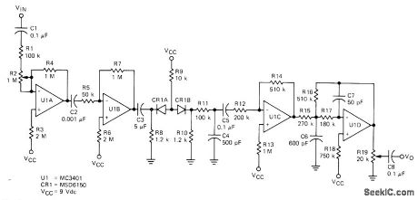
All four sections of Motorola MC3401 quad amplifier are used as intelface between high-impedance microphoneand FM modulator to provide preemρhasis response of 6 dB per octave between 300 and 3000 Hz, with 6-dB per octave rolloff beyond. lncludes amplitude limiter to prevent peak deviation of transmitter from exceeding allowed maximum. U1D forms active fillter acting with passive filter following limiter to give low-pass filter having attenuation of at least 12 dB per octave above 3 kHz.-D. Aldridge, An Economical FM Transmitter Voice Processor from a Single IC, Motorola, Phoenix, AZ, 1975. EB-57.
(View)
View full Circuit Diagram | Comments | Reading(835)
14_MHz_VFO_USING_DOUBLER
Published:2009/7/13 21:50:00 Author:May
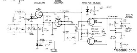
Developed for use with 20-meter low-power (QRP) transceiver. Push-push doubler avoids instability problems of 14-MHz oscillator and minimizes chirp during CW transmit periods. Uses lowdrift series-tuned Colpitts oscillator operating at 7 MHz, with source-follower buffer separating it from doubler. Adjust dynamic balance -control R1 of doubler for best output waveform purity. Capacitors marked P are polystyrene, and SM are silver mica, Article stresses importance of choosing and using components that minimize drift.-D. DeMaw, VFO Design Techniques for Improved Stability, Ham Radio, June 1976, p 10-17.
(View)
View full Circuit Diagram | Comments | Reading(2069)
SINGLE_IC_BATTERY_BACUP_MANAGER
Published:2009/7/13 21:49:00 Author:May
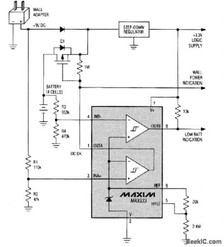
Instruments powered by a wall adapter with battery backup typically diode-OR the battery and wall-adapter connections. That arrangement carries a penalty, however-the diode in series with the battery limits the minimum voltage at which the battery can supply power. One alternative is a dual-comparator/reference IC, which monitors the battery and wall-adapter voltages with respect to its internal reference voltage. The open-drain output of comparator B (with pull-up to 3.3 V) provides a low-battery warning in the form of a low-to-high transition when battery voltage drops to 3.6 V. The open-drain output of comparator A (with pull-up to 9 V) flags low wall-cube voltage in the same way, with a warning threshold of 3.9 V. Comparator A also controls the PMOS switch Q1, which replaces the OR-connection diode in a conventional circuit. When wall power is removed, Q1 turns on and provides a low-resistance path from battery to regulator. (View)
View full Circuit Diagram | Comments | Reading(878)
600_W_HALF_WAVE
Published:2009/7/13 21:45:00 Author:May
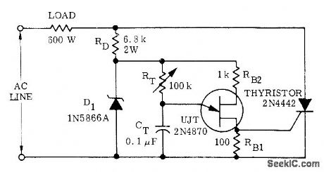
UJT serves as trigger for thyristor in circuit that provides power control for load only on positive half-cycles. Thyristor acts also as rectifier, providing variable power determined by setting of RT during positive half-cycle and no power to load during negative halfcycle.-D. A. Zinder, Unijunction Trigger Circuits for Gated Thyristors, Motorola, Phoenix, AZ, 1974, AN-413, p 3.
(View)
View full Circuit Diagram | Comments | Reading(3182)
ROCKET_LAUNCHER_IGNITER_CIRCUIT
Published:2009/7/13 21:43:00 Author:May
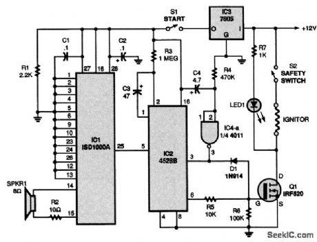
An ISD1000A chip (IC1) containing a previously recorded message is connected in a simple playback-only circuit that operates when power is supplied by closing the START switch (S1). A 7805 voltage regulator, IC3, is used to drop the 12-V input voltage to 5 V. When the audio message is completed, IC1 produces a 16-ms low output pulse at pin 25. That low output pulse is fed to the input, pin 5, of a monostable multivibrator, IC2. That IC produces a long timed output pulse at pin 6, which turns Q1 on, supplying power to the igniter and firing the rocket engine. This circuit contains several safety features. Switch S2 removes power from the igniter fuse. One gate of a 4011 quad twoinput NAND gate (IC4-a) keeps the 4528B monostable multivibrator from misfiring and igniting the rocket motor prematurely. When the Start switch is first activated, IC4-a's input goes high while C4 is charging up, and its output at pin 3 goes low, keeping IC2 from responding to any false input pulse at pin 5. IC4-a's pin 3 clamps the input of Q1 to ground, through Dl, keeping it turned off. After a few seconds, C4 is fully charged and IC4-a's output goes positive, enabling IC2 and allowing Q1 to operate. Though not shown in the figure, the inputs of the quad IC's three unused gates (IC4-b to IC4-d, pins 5, 6, 8, 9, 12, and 13) must be tied to ground. (View)
View full Circuit Diagram | Comments | Reading(1574)
INFRARED_COMMUNICATIONS_TRANSCEIVER
Published:2009/7/16 3:12:00 Author:Jessie
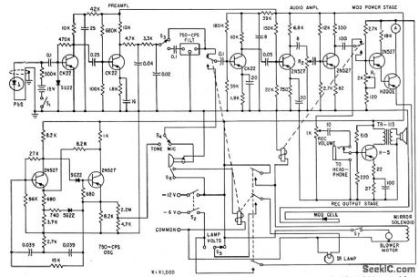
When push-to talk Switch S6 is closed amplified microphone signal modulates Infrared output of tungsten lamp. Lens gives 1° beam. When switch is released, lead sulfide cell picks up radiation from another transceiver, for driving speaker or phones through audio preamp and audio amp.-P W. Kruse and L.D. McGlauchlin, Solid-State Modulators for Infrared Communications, Electronics, 34:10, p 177-181. (View)
View full Circuit Diagram | Comments | Reading(769)
ADF_DEGREE_INDICATING_COUNTER
Published:2009/7/13 21:42:00 Author:May
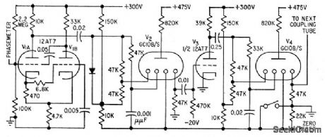
V1 is used in conventional pulse-forming circuit to drive counter V2.Each counter tube is connected to next by half of 12AT7. When first counter passes zero. Pulse at its output is fed to next conter. -J.F. Hatch and D.W.G. Byatt. Direction Finder with Automatic Readout. Electronics.32:16,p62-64 (View)
View full Circuit Diagram | Comments | Reading(595)
| Pages:167/471 At 20161162163164165166167168169170171172173174175176177178179180Under 20 |
Circuit Categories
power supply circuit
Amplifier Circuit
Basic Circuit
LED and Light Circuit
Sensor Circuit
Signal Processing
Electrical Equipment Circuit
Control Circuit
Remote Control Circuit
A/D-D/A Converter Circuit
Audio Circuit
Measuring and Test Circuit
Communication Circuit
Computer-Related Circuit
555 Circuit
Automotive Circuit
Repairing Circuit