
Index 162
PUT_CONTROLS_SCR
Published:2009/7/14 1:05:00 Author:May

Programmable unijunction transistor Q2 provides phase control for both halves of AC line voltage by triggering SCR connected across bridge. Relaxation oscillator formed by Q2 varies conduction interval of Q1 from 1 to 7.8 ms or from 21.6° to 168.5°, to give control over 97% of power available to load.-R. J. Haver and B. C. Shiner, Theory, Characteristics and Applications of the Programmable Unijunction Transistor, Motorola, Phoenix, AZ, 1974, AN-527, p 10. (View)
View full Circuit Diagram | Comments | Reading(1733)
FET_DPDT
Published:2009/7/14 1:05:00 Author:May
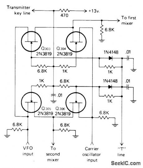
Uses FETs as switching elements for transferring VFO and carrier oscillator signals between first and second mixers of SSB transceiver. Transmitter key line is at +13 V on receive and 0 V on transmit, and T line has opposite voltages. On receive, Q304 and Q305 are pinched off by about +10 V, while Q303 and Q306 are conducting with only about +0.7 V on their gates. VFO signal then flows to first mixer and carrier oscillator to second mixer. On transmit, conditions are opposite.-J. Schultz, CQ Re-views: The Atlas 210 and 215 SSB Transceivers, CQ, May 1975, p 22-27 and 65. (View)
View full Circuit Diagram | Comments | Reading(776)
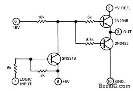
NEGATIVE_SPDT
Published:2009/7/14 1:03:00 Author:May
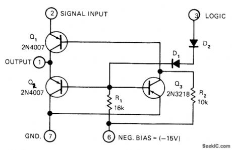
Developed for driving R/2R ladder network in D/A conveners. Signal input or reference voltage range is 0 to -12 V. With logic 0, R1 forward-biases Q2 and O3; Q2 then switches output to ground, and Q3 clamps base of Q1 to ground to keep it off. With logic 1, D1 and D2 conduct and make Q1 switch on.-J, Cohen, Solid-State Signal Switching: It's Get-ting Better All the Time, EDN Magazine, Nov. 15, 1972, p 22-28. (View)
View full Circuit Diagram | Comments | Reading(735)
SOUND_ACTIVATED_CHRISTMAS_TREE
Published:2009/7/14 1:00:00 Author:May
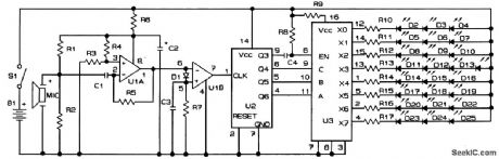
Switch S1,an ON/OFF switch,directs power from the 9-V battery to the circuit The first half of an LM358,U1A,is configured as a high-gain amplifier Resistors R3 and R4 form a voltage divider that sets the bias voltage at put 3,holding the amplifier in the Off state Resistors R1 and R2,also forming a voltage divider,set the bias point for the microphone When the audio input signal produced by the microphone exceeds the bias voltage,U1A turns on and operates as a high-gain amplifier(with the gain being set by resistor R5) Capacitor C1 couples the microphone’s signal to the amplifier’s inverting input,put 2 Resistor R6 and capacitor C2 are used as a filter network for the Op amp The second half of U1,U1B,is configured as a peak signal detector it is triggered by the negative half-cycle output of U1A Each negative half-cycle of the signal produces a positive clock signal to the input of U2,the seven-stage binary ripple counter Capacitor C3 Stores the average peak level of the input signal,and resistor R7 determines C3’s discharge tune.Integrated circuit U2 produces a binary count on its Q3 through Q6 outputs that is proportional to the frequency of the audio input signal The output of Q3 is connected,via capacitor C4,to the ENABLE pm of U3 When the input audio signal causes U2 to conduct,the relatively high-frequency output of Q3 enables U3 Resistor R3 maintains U3 In the Disabled mode Ill the absence of any audio input signal U3’s output lines,X0 through X7,are turned on and off in rapid Sequence,causing the LEDs to display a random flashing effect that is proportional to the original、al audio signal (View)
View full Circuit Diagram | Comments | Reading(1375)
ACTIVE_LOW_TRIAC_INTERFACE
Published:2009/7/14 0:58:00 Author:May
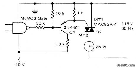
With connection shown for interface transistor Q1,typical CMOS gate triggers triac when gate output goes low, for switching of 25-W lamp load,-A. Pshaenich, Interface Techniquos Between Industrial Logic and Power Devices,″Motorola, Phoenix,AZ,1975,AN-712A,p12. (View)
View full Circuit Diagram | Comments | Reading(801)
AC_SPDT
Published:2009/7/14 0:56:00 Author:May
Complementary NPN and PNP transistors provide single-pole double-throw switching action for AC signals, as required in some digital-to-analog converter applications. Circuit switches between ground and signals of up to±5 V. Output transistor pair will toggle with unipolar drive.-J. Cohen, Solid-State Signal Switching : It's Getting Better All the Time, EDN Magazine, Nov. 15, 1972, p 22-28. (View)
View full Circuit Diagram | Comments | Reading(2283)
SINGLE_BALANCED__MIXER
Published:2009/7/15 23:26:00 Author:Jessie
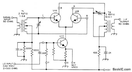
Uses RCA CA3028A differential amplifier U1 to provide conversion gain of about 30 dB for signal inputs up to 120 MHz Values of tuned circuits depend on frequency used, Unmarked resistors are on IC.-D. DeMaw, Understanding Linear ICs, QST, Feb. 1977, p 19-23. (View)
View full Circuit Diagram | Comments | Reading(1269)
ANALOG_SWITCH_PROTECTION_
Published:2009/7/14 0:54:00 Author:May
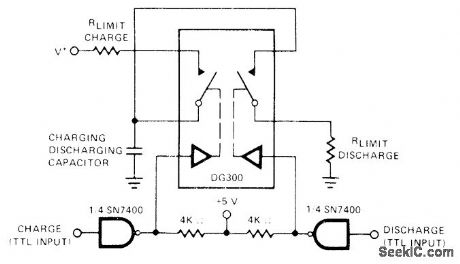
Current-limiting resistors are used in series with sections of DG300 dual analog switch to limit contact currents to 30 mA continuous or 100 mA pulsed for less than 1 ms. Values of limiting resistors depend on supply voltage used and are therefore determined by experimentation. Technique is suitable for applications in which DG300 serves for charging and discharging capacitor.- Analog Switches and Their Applications, Siliconix, Santa Clara, CA, 1976, p 7-81. (View)
View full Circuit Diagram | Comments | Reading(792)
LATCHING_SPDT
Published:2009/7/14 0:50:00 Author:May
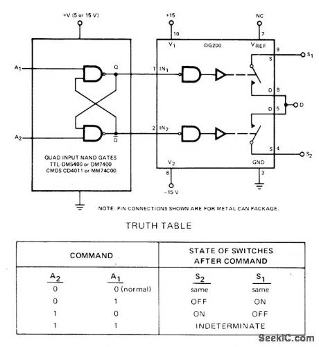
DG200 CMOS analog switch is driven through pair of NAND gates connected for logic inputs. With inputs normally low, both switches are held in predetermined states. When either input receives high command pulse, switches assume states given in truth table. Both switches are off when both inputs are held high; after release of high commands, last input to go low determines states of switches.- Analog Switches and Their Applications, Siliconix, Santa Clara, CA, 1976, p 7-69. (View)
View full Circuit Diagram | Comments | Reading(810)
DPDT_FET
Published:2009/7/14 0:47:00 Author:May
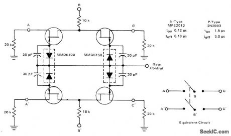
With ON resistance of several ohms and OFF resistance of thousands of megohms, drain-source channel of field-effect transistor makes ideal low-frequency switch. Transistor capacitances are detrimental to high-frequency signal isolation and limit response times.- Low Frequency Applications of Field-Effect Transistors, Motorola, Phoenix, AZ, 1976, AN-511A, p 5. (View)
View full Circuit Diagram | Comments | Reading(1078)
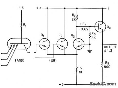
AND_LOGIC_GATE
Published:2009/7/16 1:50:00 Author:Jessie
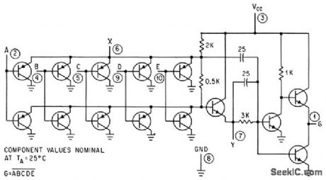
And/or gate using pnp input transistors and npn output transistors is followed by three-transistor inverting output stage. Gate has fan-in of 5.-C. R. Cook, Jr., and B. M. Martin, New semiconductor Networks Reduce System Complexity, Electronics, 37:2, p 25-29. (View)
View full Circuit Diagram | Comments | Reading(616)
BRIDGE_GATE_TEST_CIRCUIT
Published:2009/7/16 1:49:00 Author:Jessie
Two-state a-c bridge having biased tunnel-diode in one arm can be used as gale when balanced in one of its stable states.-F. W. Kantor, Tunnel-Diode Gale has Subnanosecond Rise Time, Electronics, 35:15, p 62-64. (View)
View full Circuit Diagram | Comments | Reading(647)
TEACHING_MACHINE_REWARD_GATE
Published:2009/7/16 1:48:00 Author:Jessie
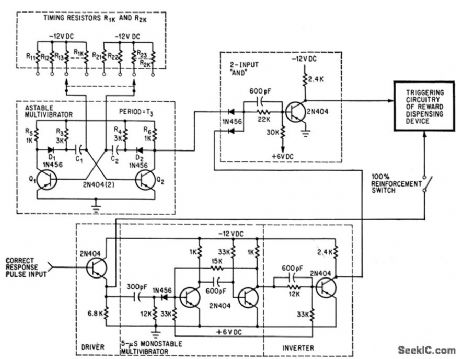
Astable and monostable multivibrators feed and gale that triggers reward-dispensing device(such as candy dispenser) when number of correct answers exceeds preset percentage of random Probability.Circuit may also give 100% reinforcement for correct response but with candy reward only at spaced intervals.-G. S. Pennington, Jr. and J. A. Boehm, III, Gate Varies Rewards from Teaching Machine, Electronics, 39;10, p 92-93. (View)
View full Circuit Diagram | Comments | Reading(673)
MULTIEMITTER_TRANSISTOR_AND_OR_LOGIC
Published:2009/7/16 1:48:00 Author:Jessie
Circuits may be coupled either directly or by multi-emitter transistor and gates. Components show promise for integrated circuits.-P. M. Thompson, Logic Principles for Multi-emitter Transistors, Electronics, 3637, p 25-29. (View)
View full Circuit Diagram | Comments | Reading(876)
FAST_ON_AND_OFF
Published:2009/7/14 0:42:00 Author:May
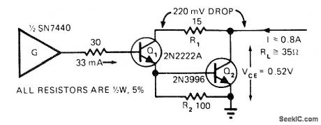
Driver Q1 is low-power device with fast switching time, while power transistor Q2 handles power dissipation and amperes of current being switched. Used in TTL circuits requiring fast solid-state switches having known and repeatable switching times. Cur-rent reaches maximum in about 50 ns.-C. Venditti, Fast Power Switch Self-Corrects for Degradation, EDN Magazine, Jan. 20, 1975, p 59-60. (View)
View full Circuit Diagram | Comments | Reading(733)
ULTRALINEAR_SWEEP
Published:2009/7/14 0:41:00 Author:May
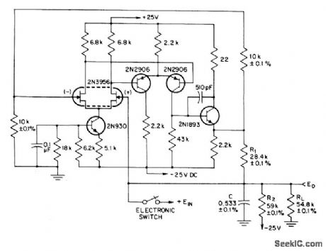
Designed to generate horizontal and vertical sweep signals for military radar system, Linearity was so good that deviations could not be measured. With Ein positive as shown, circuit gives negative going sweep. Reverse input polarity to get positive-going sweep. Circuit is immune to short-circuits.-R. C. Scheerer, Designing Linear Sweep Generators, EDN|EEE Magazine, July 1, 1971, p 39-42. (View)
View full Circuit Diagram | Comments | Reading(1066)
RAMP_FROM
Published:2009/7/14 0:40:00 Author:May
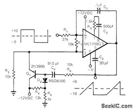
10 V-Based on use of integrating opamp to generate triangle wave from square wave. Circuit goes one step further by convening triangle to ramp function having predetermined negative starting level of -10V. When square-wave input signal changes in polarity from positive to negative, output of circuit begins to go positive as ramp function and C4 charges with output voltage. When input changes from negative to positive and output begins to go negative, Q1 conducts and drives noninverting input of opamp negative. Since square-wave input is positive at this time, opamp output is forced to go negative at its slew rate. Output then remains negative until square-wave input switches in negative direction for repeating cycle.-L. Wing, Op Amp and One Transistor Produce Ramp Function, EDN Magazine, Nov. 15, 1972, p 49. (View)
View full Circuit Diagram | Comments | Reading(1259)
DIGITAL_RAMP_1
Published:2009/7/14 0:39:00 Author:May
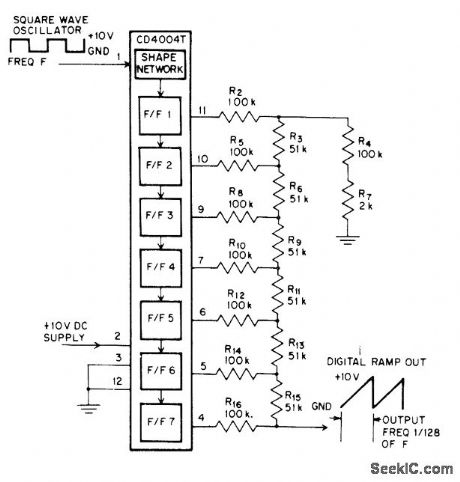
RCA CD4004T IC, internally connected as ripple counter, provides flip-flop outputs corresponding to number of binary bits loaded into single input 1. Frequency range of counteris DC to 2.5 MHz, making it ideal for low-frequency operation. With R-2R ladder connected to flip-flop outputs, input square wave gives digitally stepped ramp at ladder output, with ramp frequency equal to 1/128 of input frequency.-W. E. Peterson, Digital Ramp Generator, EEEA Magazine, Jan. 1971, p 64-65. (View)
View full Circuit Diagram | Comments | Reading(1059)
INVERTING_AMPLIFIER_GIVES_COMPLEMENT_OUTPUT
Published:2009/7/16 1:48:00 Author:Jessie
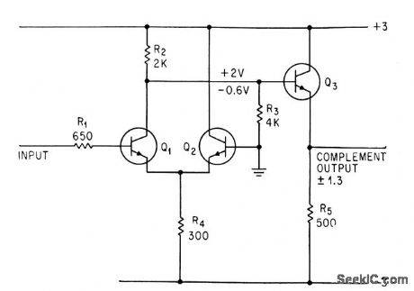
Only one transistor has isolated collector, so only three isolated lands are needed for integrated-circuit construction.-P. M. Thompson, Logic Principles for Multiemitter Transistors, Electronics, 36137, p 25-29. (View)
View full Circuit Diagram | Comments | Reading(594)
VARIABLE_START_STOP
Published:2009/7/14 0:37:00 Author:May
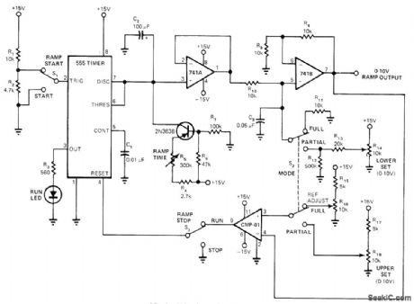
Ramp generator can be operated either in full ramp mode, with out-put sweeping from 0 to +10 V, or partial ramp mode in which output sweeps between adjustable starting point and adjustable stopping point. R5 selects time period in both modes. Ramp is reset automatically when output reaches preset voltage limit. Values shown for C2 and R5 give 100-s charge time, but changing R5 to 1 megohm increases charge period to 7 min. S3 stops ramp and resets circuit at any point in ramp cycle.-D. Dantuono, Ramp Generator Features Variable Start/Stop Points, EDN Magazine, April 20, 1978, p 130 and 132. (View)
View full Circuit Diagram | Comments | Reading(1098)
| Pages:162/471 At 20161162163164165166167168169170171172173174175176177178179180Under 20 |
Circuit Categories
power supply circuit
Amplifier Circuit
Basic Circuit
LED and Light Circuit
Sensor Circuit
Signal Processing
Electrical Equipment Circuit
Control Circuit
Remote Control Circuit
A/D-D/A Converter Circuit
Audio Circuit
Measuring and Test Circuit
Communication Circuit
Computer-Related Circuit
555 Circuit
Automotive Circuit
Repairing Circuit