
Index 174
10_Hz_100_kHz_RAMP
Published:2009/7/13 6:14:00 Author:May
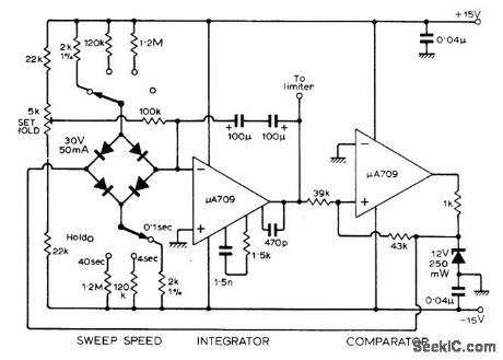
Uses Miller integrator switched at selected rate by IC comparator in feedback loop. Ramp circuit was developed to drive FETs serving as voltage-dependent resistances in Wien-bridge oscillator of AF sweep generator. Article gives all circuits and construction details. Sweep linearity is better than 15% for all four ranges, covering 10 Hz to 100 kHz. For greatest accuracy, use 40-s sweep time; 4-s sweep is for long-persistence CRT, and 0.1-s sweep can be used only on upper three ranges.-F. H. Trist, Audio Sweep Generator, Wireless World, July 1971, p 335-338. (View)
View full Circuit Diagram | Comments | Reading(1128)
30_Hz_SAWTOOTH
Published:2009/7/13 6:14:00 Author:May

Uses neons as relaxation oscillator for producing sawtooth wave required for monitor scope of SSB transmitter. Rate at which C1 charges depends on its value and those of R2 and R3. When C1 charges to breakdown voltage of neon string, around 70 V per tube, neons fire and C1 discharges through them. C1 then starts charging again, to give sawtooth output. Voltage source should be about 500VDC, and R1 at least 500K. For greater sweep width, increase number of neons in series.-D. Schmarder, A Simple Sweep Generator for Monitor Scopes, 73 Magazine, Feb. 1974, p 32. (View)
View full Circuit Diagram | Comments | Reading(741)
FAST_FLYBACK_2_V_SAWTOOTH
Published:2009/7/13 6:13:00 Author:May
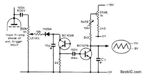
Simple modern time-base circuit using transistors can be added to old oscilloscopes that have only a synchronized free-running sweep. Size of CT determines sweep rate. When timing capacitor CT charges to breakdown voltage of reverse biased BC107B, capacitor is quickly discharged until voltage drops about 2 V and transistor assumes its high-resistance state again for start of next sweep.-K. Padmanabhan, Timebase Circuit, Wireless World, June 1974, p 196. (View)
View full Circuit Diagram | Comments | Reading(713)
ADJUSTABLE_NONLINEAR_RAMP
Published:2009/7/13 6:12:00 Author:May
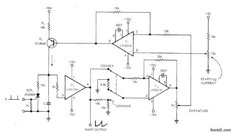
Circuit provides predistortion of sweep with concavity or convexity as required to compensate for nonlinearity of circuit being driven, Q1 operates as constant-current source that provides current proportional to voltage difference between ±15 V supply and base voltage of Q1. Ramp output is linear when wiper of curvature pot is set to minimum position (ground). Period of ramp is same as that of trigger impulses that gate SCR on. Circuit uses DC coupling, avoiding need for large coupling capacitors. With 0.22μF for C, period is 6 ms.-H, Olson, Ramp Generator Has Adjustable Nonlinearity, EDN Magazine, May 20, 1973, p 85 and 87. (View)
View full Circuit Diagram | Comments | Reading(817)
02_20000_Hz_VOLTAGE_CONTROLLED_RAMP
Published:2009/7/13 6:11:00 Author:May
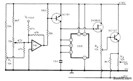
With values shown, frequency of ramp can be varied over range of about 20 kHz by changing DC input voltage. Lowest frequency is set by R1. Adjust R2 to make average output 0V, and set desired output level with R3. Uses 555 IC timer as astable MVBR, with charge current being supplied by transistor. Voltage/frequency relationship is logarithmic, making oscillator suitable for use in sound synthesizers.-J. L. Brice, Voltage-Controlled Ramp Generator, Wireless World, June 1976, p 72. (View)
View full Circuit Diagram | Comments | Reading(976)
CRYSTAL_CONTROLLED_SUPERREGENERATIVE
Published:2009/7/16 2:54:00 Author:Jessie

Two high-frequency transistors connected as 20-kHz MVBR provide switching action at same rate for RF oscillations generated in crystal feedback path. Received AM signal induced in tank circuit of C1 will modulate exact switching point of circuit at rate directly proportional to modulation component of received signal. Choose L1, C1, and crystal for frequency desired. If at 10 MHz, standard WWV time broadcasts can be picked up. -I. Math, Math's Notes, CQ, Sept. 1972, p 36-37.
(View)
View full Circuit Diagram | Comments | Reading(2431)
LOGIC_CONTROLLED_RAMP_RATE
Published:2009/7/13 6:10:00 Author:May

Bidirectional linear ramp generator uses FET switch to slow ramp. With FET off, fast ramp has duration of 100 ms. With FET on, slow ramp is 1 s.-R.W. Currell, Linear Bidirectional Ramp Generator, EDN|EEE Magazine, Nov. 1, 1971, p 50-51. (View)
View full Circuit Diagram | Comments | Reading(1392)
LOGIC_LEVEL_CONVERTER
Published:2009/7/13 6:10:00 Author:May
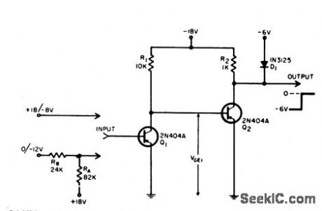
Converts from +18/-8V logic levels of some frequency converters and other digital test equipment to commonly used 0/-6V logic levels of datalogging system.-C. M. Jackson, Logic-Level Converter, EEE, 12:9, p61. (View)
View full Circuit Diagram | Comments | Reading(1608)
REFERENCE_VOLTAGE_FOR_DIGITAL_CONVERTER
Published:2009/7/13 6:08:00 Author:May
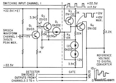
Rectifies speech signals over 30.db range, and allows charge of memory capacitor to rise in millisec when speech input is applied, to form reference input voltage to digital converter for ratio quantizing unit.-J. D. Howells, Better Speech Quantizing for Pulse-Code Modulation, Electronics, 35:48, p 84-88. (View)
View full Circuit Diagram | Comments | Reading(1336)
RESONANT_FLUXGATE_MAGNETOMETER
Published:2009/7/13 6:06:00 Author:May
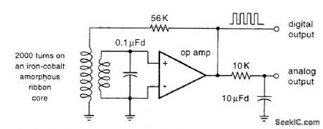
The core will get switched in the out of saturation. The output duty cycle varies in proportion to single-axis field strength and direction. The high-level output square wave is easy to interface to a PIC or other microcontroller. (View)
View full Circuit Diagram | Comments | Reading(1850)
450_MC_TO_30_MC
Published:2009/7/13 6:05:00 Author:May
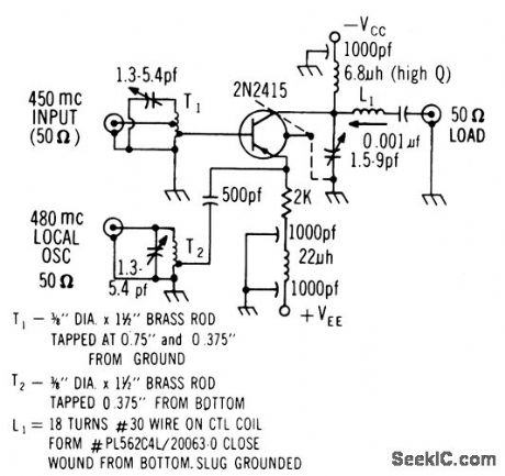
With local oscillator feeding 1 mw,conversion gain is 15 db and noise figure 10 db.With 2N2415 r-f stage ahead of mixer.combined power gain is 25db and noise figure 6 db.-Texas instruments Inc, Solid-State communications. McGawHill,N,Y.1966,p302. (View)
View full Circuit Diagram | Comments | Reading(588)
LINEAR_RAMP
Published:2009/7/13 6:04:00 Author:May
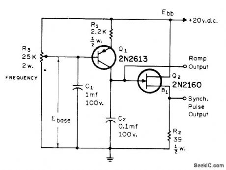
Free-running ramp generator has excellent linearity and repetition rate independent of supply voltage. C2 is charged at constant current through a, and is discharged by Q2. R2 provides sync pulse during retrace. Repetition rate of ramp is controlled by R3, from about 100 to 4000 Hz. Output voltage is 10 V P-P, and sync pulse amplitude is 5 V P-P.-J. J. Nagle, Voltage Independent Ramp Generator, CQ, Sept. 1972, p 61 and 98. (View)
View full Circuit Diagram | Comments | Reading(0)
BIDIRECTIONAL_RAMP
Published:2009/7/13 6:04:00 Author:May
Originally used to vary reference voltage for DC servomotor to control acceleration and deceleration. R2 and C1 determine ramp rate, while R1 controls ramp amplitude. With values shown, output takes n s to ramp from 0 to 10 V.-R. W. Currell, Linear Bidirectional Ramp Generator, EDN|EEE Magazine, Nov. 1, 1971, p 50-51. (View)
View full Circuit Diagram | Comments | Reading(846)
15_RANGE_SWEEP
Published:2009/7/13 6:03:00 Author:May
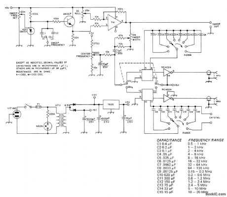
Serves for adjusting tuned circuits, aligning IF strips, and checking filter characteristics. Uses Motorola MC4024 IC containing two separate voltage-controlled MVBRs with output buffer for each. Frequency of oscillation is determined primarily by single switch-selected external capacitor that gives choice of 15 frequency ranges, with frequency within each range varied by applying DC control voltage to one pin of IC. For 3.5-5 V of control voltage, linearity is good. Output waveform is 4 V P-P at lower frequencies, becoming triangular at higher frequency ranges. HEP S9001 programmable UJT generates sweep signal. Switch gives choice of 100 Hz or 1 kHz sweep. Buffer and 741 opamp then give exponential sweep from about -1 to +1 V after DC level is set to 0 by 25K pot, for horizontal input of CRO. Sweep signal is also fed to MVBRs through controls giving independent width and center frequency adjustments. Diodes are 1-A 50-PIY silicon, T1 is 6.3 V at 1 A.-W. C. Smith, An Inexpensive Sweep-Frequency Generator, QST, Oct. 1976, p 17-19. (View)
View full Circuit Diagram | Comments | Reading(1404)
PREAMP_WITH_TONE_CONTROLS_1
Published:2009/7/13 6:00:00 Author:May
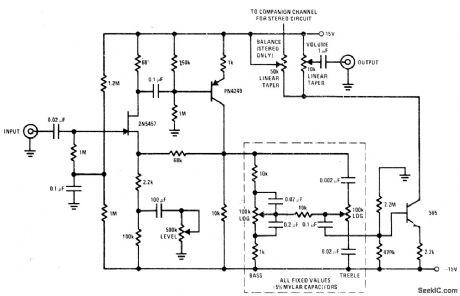
Input stage is JFET having high input impedance and low noise. Circuit parameters are not critical, yet harmonic distortion level is less than 0.05% and S/N ratio is over 85 dB. Tone controls allow 18 dB of cut and boost. Input of 100 mV gives 1-V output at maximum level. Identical preamp is used for other stereo channel.- FET Data-book, National Semiconductor, Santa Clara, CA, 1977, p 6-26-6-36. (View)
View full Circuit Diagram | Comments | Reading(918)
D_C_TO_D_C
Published:2009/7/13 6:00:00 Author:May
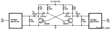
Free-running multivibrator (250 kc) generates unidirectional square waves having amplitude of d-c input voltage. R-C circuit at output blocks average value of unidirectional pulse,and standard diode-capacitor voltage multiplier boosts output voltage to desired new value.-A. J. Durocher, D.c Voltage Converter Needs No Transforme, Electronics, 37:28, p 64-65. (View)
View full Circuit Diagram | Comments | Reading(839)
FM_HISS_LIMITER
Published:2009/7/13 5:59:00 Author:May
Uses low-pass filter to remove noise sometimes heard with weak passages during stereo reception of FM stations. FET driven by output of amplifier or tuner is used to switch low-pass filter into operation rather than switching over to mono. Based on fact that the hiss is an antiphase effect that can be removed with little detriment to overall signal.-G. Hibbert, Stereo Noise Limiter Improvement, Wireless World, March 1976, p 62. (View)
View full Circuit Diagram | Comments | Reading(1147)
3O_MC_TO_55_MC
Published:2009/7/13 5:55:00 Author:May
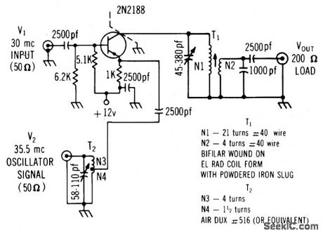
Single transistor serves as mixer to give 5.5-Mc i-f signal from 30-Mc signal input and 35.5.-Mc oscillator input.Output is 100 mv for 10-mv signal input, with 630-mv oscillator signal.-Texas Instruments Inc. Solid-State Communications, McGraw-Hill, N.Y. 1966, p300. (View)
View full Circuit Diagram | Comments | Reading(782)
VOLTAGE_TO_FREQUENCY_CONVERTER
Published:2009/7/13 5:51:00 Author:May
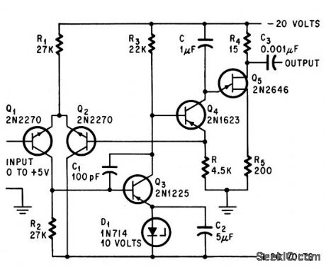
Q4 supplies charging current for C in relaxation oscillator Q5. Differential amplifier Q1-Q2 compares charging current with input voltage. Difference signal, amplified by Q3, controls charging current through Q4 and thus makes output frequency proportional to input voltage. For 0 to +5V input, output is 0 to 100 cps with 0.1% linearity.-W. H. Voelker, Transistor Circuit Converts Voltage to Regulated Frequency, Electronics, 37:29, p73-74. (View)
View full Circuit Diagram | Comments | Reading(0)
PULSE_HEIGHT_TO_TIME_CONVERTER
Published:2009/7/13 5:49:00 Author:May
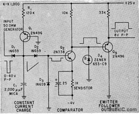
Output width is proportional to input height. Last stage of constant-current charge circuit can be eliminated if output impedance can be high.-D. N. Carson and S. K. Dhawan, Data Conversion Circuits for Earth Satellite Telemetry, Electronics, 33:3, p82-84. (View)
View full Circuit Diagram | Comments | Reading(810)
| Pages:174/471 At 20161162163164165166167168169170171172173174175176177178179180Under 20 |
Circuit Categories
power supply circuit
Amplifier Circuit
Basic Circuit
LED and Light Circuit
Sensor Circuit
Signal Processing
Electrical Equipment Circuit
Control Circuit
Remote Control Circuit
A/D-D/A Converter Circuit
Audio Circuit
Measuring and Test Circuit
Communication Circuit
Computer-Related Circuit
555 Circuit
Automotive Circuit
Repairing Circuit