
Index 169
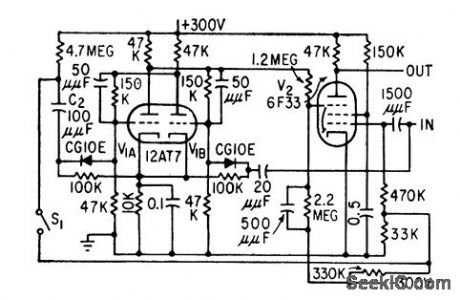
INVERTER_LIMITER
Published:2009/7/13 21:30:00 Author:May
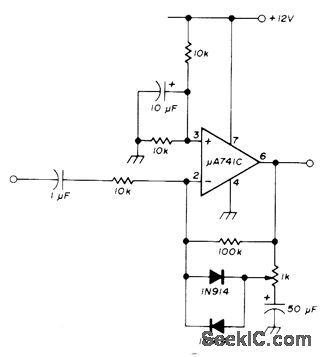
Developed for direct-conversion receivers that lack AGC, to provide limiting for CW reception. Below adjustable limiting threshold, amplifier is linear with voltage gain of 10. When output is high enough for silicon diodes to conduct, gain drops below unity.Amplifier should be preceded by several sections of filtering and followed by single-section low-pass filter to eliminate harmonic distortions generated in limiting process.-W. Hayward, Simple Active Filters for Direct-Conversion Receivers, Ham Radio, April 1974, p 12-15. (View)
View full Circuit Diagram | Comments | Reading(650)
10_CHANNEL_SCANNER
Published:2009/7/13 21:29:00 Author:May
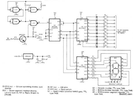
Designed for Regency HR-212 2-meter transceiver but can be adapted for other transceivers,Features include automatic stop, start, and large LED 7-segment readout. Diodes D1-D10 prevent transceiver voltages from reaching scanner circuit. Squelch voltage input of 2N3053 is taken from transceiver. S1-S10 are used to switch out channels not monitored. Wires going to chokes in HR-212 should be connected to choke leads going to channel switch.-A. Little, 10-Channel Scanner for the Regency HR-212, QST, Feb. 1978, p 37. (View)
View full Circuit Diagram | Comments | Reading(1462)
SIMPLE_SCANNER_CONVERTER
Published:2009/7/13 21:29:00 Author:May

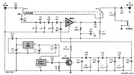

This circuit can be powered from any 9- to 12-Vdc source, including a good alkaline 9-V battery.Switch S1 either puts the unit into its Bypass mode, where a scanner connected to J3 will receive its normal signals, or applies power to the circuit and down-converts all 800- to 950-MHz signals as follows: At the heart of the circuit is OSC1, a 40-MHz oscillator module. Transistor Q1 amplifies the oscillator's output, which is then bandpass filtered four times so that only the tenth harmonic at 400 MHz is presented to the input of U1, a Mini Circuits MAR1 wideband UHF/VHF amplifier. Signals from an antenna connected to J2 are high-pass filtered by capacitors C4 to C7 in conjunction with inductors L2 to L4. Those inductors are etched into the tracings on the PC board, making the exact PC board layout a necessity if the circuit is to function. Mixer U1 amplifies and mixes the two inputs-signals between800 and 950 MHz and the 400-MHz local oscillator-and passes the 400- to 550-MHz output to J3. This converter is not suitable for areas where signal strength is low or areas where a large number of strong signals are present, as no RE stage is used and little input filtering is used be-fore the mixer, making this circuit prone to spurious responses. (View)
View full Circuit Diagram | Comments | Reading(766)
“BAT_BAND”CONVERTER
Published:2009/7/13 21:27:00 Author:May
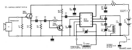
The full circuit diagram of the bat-band converter is shown. All components, with the exception of the transducer (X1), the ON/OFF switch, and the ferrite rod antenna, are surface-mount devices (SMDs). The signals from X1 are very small (microvolts, rather than millivolts). A low-noise FET input stage, TR1, has minimal loading effect on X1 and provides a low-impedance source for the passive high-pass filter. This simple filter consists of capacitors C1 and C2 and resistor R3. It attenuates signals below about 15 kHz, but the rolloff is very gradual. Mid-range and lower-frequency audio is strongly reduced. The falling sensitivity of transducer X1 further limits the audio frequencies reaching the mixer IC1. Despite this level of attenuation, a little audio still gets through the system, but it has no effect on the ultrasonic operation. When the receiver is tuned close to the 1-MHz local oscillator, a little audio feedback will be heard. This is a real help with tuning in because it readily identifies the low-frequency end of the bat band. The transistor TR2 is a low-noise amplifier, and the SMD-type BSX70H works well in this circuit. IC1 is a double-balanced mixer and Colpitts oscillator in one package. The signal inputs at pin 1 and pin 2 are used in unbalanced mode, with pin 2 decoupled by capacitor C4. (View)
View full Circuit Diagram | Comments | Reading(844)
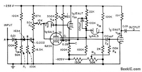
ZERO_CROSSING_SWITCH_FOR_HEART_SOUNDS
Published:2009/7/16 2:20:00 Author:Jessie
Active filter with three amplifiers provides output pulse for opening sliding gate at instant when heart sound being monitored is zero. Filter has sharp cutoff above highest-frequency heart sound (600 cps.)-R. Weiss, Heart-Sound Discriminator Simplifies Medical Diagnosis, Electronics, 34:24, p 52-55. (View)
View full Circuit Diagram | Comments | Reading(664)
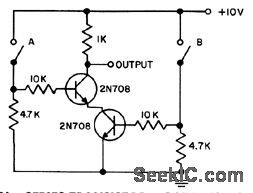
SINGLE_POSITIVE_PULSE_GATES_SINE_WAVE_SIGNAL
Published:2009/7/16 2:19:00 Author:Jessie
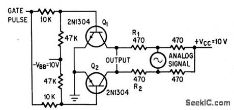
Two transistors act as balanced shorting switch, eliminating pedestal effects that normally necessitate dual-polarity gate pulses for analog signal. Positive 10-V pulse saturates both transistors, thereby grounding both output terminals to give isolation from input signal. Analog signal being gated can be as low as 5-mv rms.-L. E. Frenzel, Jr., Gate Circuit Eliminates Pedestal Effects, Electronics, 37:15, p 77. (View)
View full Circuit Diagram | Comments | Reading(683)
PUMPED_TUNNEL_DIODE_LOGIC_GATES
Published:2009/7/16 2:18:00 Author:Jessie
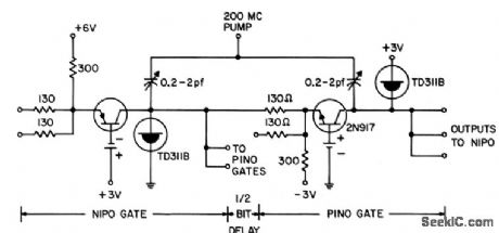
Shows method of interconnecting negative-input positive-output gate with positive-input negative-output gate for high-speed computer logic.- Transistor Manual, Seventh Edition, General Electric Co., 1964, p 370. (View)
View full Circuit Diagram | Comments | Reading(832)
AND_GATE
Published:2009/7/16 2:17:00 Author:Jessie
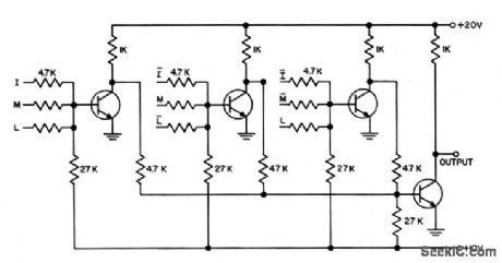
Uses nor logic with inversion.- Transistor Manual, Seventh Edition, General Electric Co., 1964, p 179. (View)
View full Circuit Diagram | Comments | Reading(1824)
MOS_DRIVE_FOR_TRIAC
Published:2009/7/13 21:26:00 Author:May
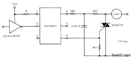
Circuit uses one section of MC75492 hex buffer to boost 0.5-mA output of CMOS logic gate to 10 mA required for LED at input of Motorola MOC3011 optically coupled triac driver. When MOS input goes high, optoisolator provides output voltage for triggering triac that controls AC load. R is 220 ohms for 5-V supply and 600 ohms for 10-V supply. For 15 V, use MC14049B buffer and 910 ohms for R.-P. O'Neil, Applications of the MOC3011 Triac Driver, Motorola, Phoenix, AZ, 1978, AN-780, p 4. (View)
View full Circuit Diagram | Comments | Reading(1878)
15_W_ADD_ON
Published:2009/7/13 21:26:00 Author:May
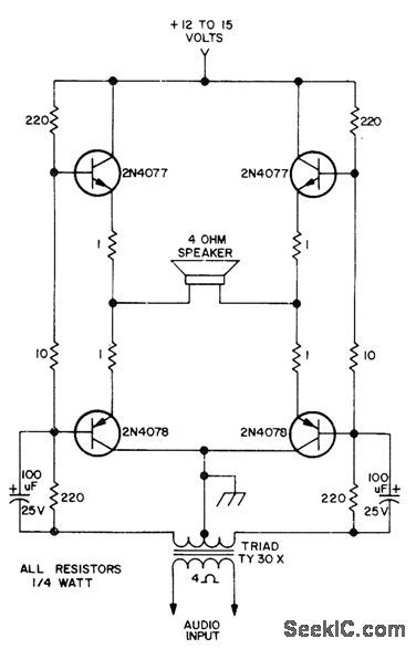
Increases usual 1-W audio output of transceiver to up to 15 W. Loudspeaker can be 8-ohm unit, but output will be somewhat reduced. -P. Bunnell, More Fun with the IC-230, 73 Magazine, May 1975, p 45-46 and 48. (View)
View full Circuit Diagram | Comments | Reading(700)
ONE_SHOT_LOGIC_CONTROLS_TRANSMISSION_GATE
Published:2009/7/16 2:17:00 Author:Jessie
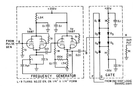
Frequency generator, activated by negative pulse at A, generates 32-Mc burst in which number of cycles depends on input pulse width. Pushbutton-controlled one-shot logic allows diode transmission gate lo pass first complete 32-Mc burst occurring after pushbutton is actuated, after which gate is closed. One-shot has sync connection to pulse generator.-V. Kenn, One-Shot Gating Circuit Generates Sinewaves lot Testing Counters, Electronics, 34:23, p 114-116. (View)
View full Circuit Diagram | Comments | Reading(877)
HARD_LIMITING_OPAMP
Published:2009/7/13 21:25:00 Author:May
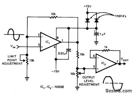
Based on limited output swing of opamp. Single pot adjusts both positive and negative limit points. First opamp produces limiting. Second opamp serves as voltage follower for isolating attenuator and redueing output impedance. Matching of output between limit points is within about 100 mV at output level of 2 V P-P. Opamps specified are adequate for 3-kHz bandwidth.-E. E. Bames, Ease Hard-Limiter Design with Op Amps, EDN Magazine, Aug. 5, 1975, p 76. (View)
View full Circuit Diagram | Comments | Reading(1734)
55_MC_CRYSTAL_OSCILLATOR_GATE
Published:2009/7/16 2:13:00 Author:Jessie
Provides train of pulses to be recd by 7-digit binary counter. Number of pulses in train depends on width of gate pulse received from gate amplifier, and is proportional to amplitude of data input pulse.-W. W. Grannemann et al, Pulse-Height-to-Digital Signal Converter, Electronics, 33:2, p 58-60. (View)
View full Circuit Diagram | Comments | Reading(497)
COMBINATION_GATE_AND_ONE_SHOT
Published:2009/7/16 2:12:00 Author:Jessie
Uses two four-layer switching diodes, and draws no current from source except during gate pulse. Can also be used as one-shot. Width of pulse depends on supply voltage and R5-C2.-R. E. Amsterdam, Gate/One. Shot Uses Four-Layer Diodes, EEE, 12:12, p 58-60. (View)
View full Circuit Diagram | Comments | Reading(543)
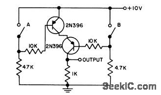
NPN_SERIES_TRANSISTOR_GATE_1
Published:2009/7/16 2:12:00 Author:Jessie
Circuit is and gate if closing of switch is an input. Circuit is or gate if opening of switch is an input. Provides phase inversion of input.- Transistor Manual, Seventh Edition, General Electric Co., 1964, p 176. (View)
View full Circuit Diagram | Comments | Reading(680)
PNP_SERIES_TRANSISTOR_GATE
Published:2009/7/16 2:11:00 Author:Jessie
Circuit is or gate if closing of switch is an input. Circuit is and gate if opening of switch is an input. Provides phase inversion of input.- Transistor Manual, Seventh Edition, General Electric Co., 1964, p 176. (View)
View full Circuit Diagram | Comments | Reading(1244)
SYNCHRONIZED_GATE
Published:2009/7/16 2:10:00 Author:Jessie
Continuous train of pulses is applied to control grid of gating tube. When S1 is closed, next pulse in train opens gate, then shuts gate after itself.-J. K. Goodwin, Time and Pulses Control Gates, Electronics, 32:3, p 72-73. (View)
View full Circuit Diagram | Comments | Reading(688)
TWIN_PHANTASTRON
Published:2009/7/16 2:10:00 Author:Jessie
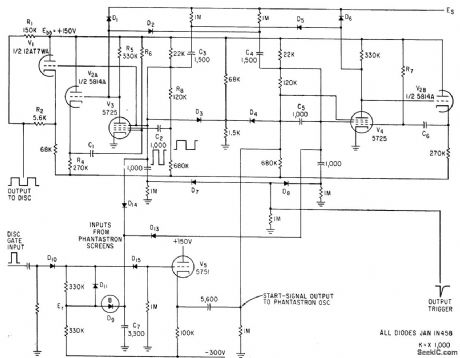
Frequency of free.-running twin-phantastron oscillator V3-V4 varies with controlled voltage ES (upper right). V5 gates starting pulses to phantastron when-ever it fails to oscillate. Used to generate train of pulses that continues in synchronism with incoming video data even when sync pulse is missing or below noise level-W. C. Whitworth, Plate Voltage Control of Phantrastron Frequency, Electronics, 34:6, p 73-74. (View)
View full Circuit Diagram | Comments | Reading(1473)
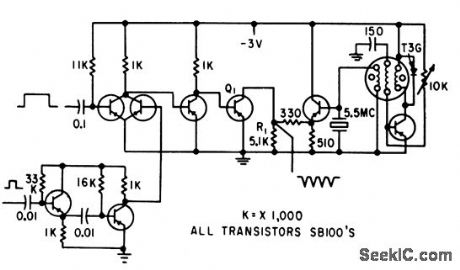
GAIING_WITH_VARICAPS_AND_TRIODES
Published:2009/7/16 2:10:00 Author:Jessie
Gives 100-db on-off ratio of 5.5-Mc signal, using small-amplitude positive-pulse gate (about 4 V) with two dual triodes and four tuned circuits with varicaps in each. Tuned circuits are shifted from parallel to series resonance by gating signal.-Gating with Varicaps, Electronic Circuit Design Hand-book, Mactier Pub. Corp., N.Y., 1965, p 211. (View)
View full Circuit Diagram | Comments | Reading(657)
SELF_SETIING_PULSE_PATTERN_GATE
Published:2009/7/16 2:09:00 Author:Jessie
Picks out pulses transmitted at fixed repetition frequency, in presence of random noise, to improve reliability of ionospheric pulse transmitter-receiver synchronizing link by factor of 50.-E. R. Schmerling, Self-Setting Servo Gate, Electronics, 31:3, p 71.
(View)
View full Circuit Diagram | Comments | Reading(595)
| Pages:169/471 At 20161162163164165166167168169170171172173174175176177178179180Under 20 |
Circuit Categories
power supply circuit
Amplifier Circuit
Basic Circuit
LED and Light Circuit
Sensor Circuit
Signal Processing
Electrical Equipment Circuit
Control Circuit
Remote Control Circuit
A/D-D/A Converter Circuit
Audio Circuit
Measuring and Test Circuit
Communication Circuit
Computer-Related Circuit
555 Circuit
Automotive Circuit
Repairing Circuit