
Index 179
PREAMP_FOR_INFRARED_MINE_DETECTOR
Published:2009/7/16 3:27:00 Author:Jessie
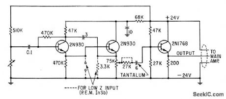
Lead telluride cell cooled with dry ice, with infrared input chopped at 200 cps by fan motor, feeds three-transistor preamp that provides output at 200 ohms to remote R-C tuned main 200-cps amplifier.-W. E. Osborne, Infrared Mine Detector a Reality, Electronics, 36:31, p 54-58. (View)
View full Circuit Diagram | Comments | Reading(1495)
25_500_kHz_TO_35_4_MHz
Published:2009/7/16 3:27:00 Author:Jessie
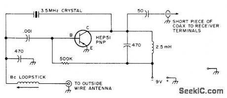
When receiver is tuned to 3.5 MHz and converter is peaked for loudest signal, combination is tuning 25.kHz range. With receiver tuned to 4 MHz converter gives coverage at 500 kHz.--Circuits, 73 Magazine, May 1977, p 19. (View)
View full Circuit Diagram | Comments | Reading(807)
IR_WIDTH_GAGE_TRANSLATOR
Published:2009/7/16 3:26:00 Author:Jessie
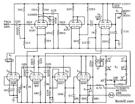
Combined signal output from main amplifier of infrared gage triggers bistable mvbr V7, output of which is rectangular pulse whose width is proportional to steel strip width. Pulse is clamped and amplified by V8 and passed to comparator V9, which provides output proportional in amplitude to width of input pulse.-F. J. Dunks, Infrared Gage Measures Hot Steel Strip Width, Electronics, 33:43, p 65-67. (View)
View full Circuit Diagram | Comments | Reading(643)
INFRARED_HOT_ENGINE_DETECTOR_1
Published:2009/7/16 3:25:00 Author:Jessie
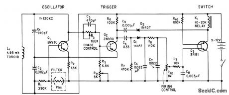
Hot-engine alarm using only two transistors and an car resets parking meter to zero when lead sulfide infrared detector senses engine heal as parked car starts. Circuit combines Colpitts oscillator with Schmitt trigger.-W. E. Osborne, Farewell To Free Time On City Parking Meters, Electronics, 37:32, p 72.-74. (View)
View full Circuit Diagram | Comments | Reading(1248)
FREQUENCY_PERIOD_EVENT_TIME
Published:2009/7/13 4:43:00 Author:May
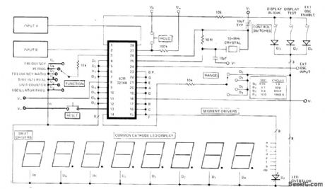
Universal counter with 10-MHz maximum frequency pro-vides multiple functions with minimum number of components. Range of time period measure-ments is 0.5 μs to 10 s. Includes 10-MHz crystal oscillator, multiplex timing with inter digit and leading-zero blanking, as well as overflow indication. Decimal position is selectable. Eight-digit multiplexed LED display outputs of IC can switch up to 250 mA per digit for handling large displays. Maximum supply voltage is 6 V.-Low Cost Universal Counter Performs Wide Range of Functions, Computer Design, Aug. 1978, p 168 and 170. (View)
View full Circuit Diagram | Comments | Reading(929)
PIEZOELECTRIC_DRIVER_CIRCUIT
Published:2009/7/13 4:42:00 Author:May
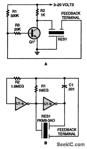
Three-terminal piezoelectric elements are typically driven by transistor circuits (A) or logic gates (B). (View)
View full Circuit Diagram | Comments | Reading(1534)
ELECTRICAL_SYSTEM_ANALYZER
Published:2009/7/13 4:41:00 Author:May
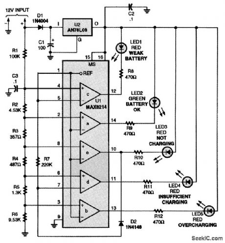
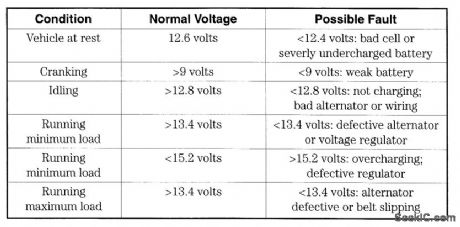
The automotive electrical diagnostic system is built around a Maxim MAX8214ACPE five-stage voltage comparator, which contains a built-in 1.25-V precision reference and on-board logic that allows the outputs of two of the comparators to be inverted. (View)
View full Circuit Diagram | Comments | Reading(824)
DIGITAL_COUNTING_DEMONSTRATOR
Published:2009/7/13 4:41:00 Author:May

555 timer serves as dock for driving RS7490 decade counter feeding RS7447 BCD to 7-segment decoder that drives 7-segment digital display. R1 is adjusted to give clock frequency that makes display cycle slowly through digits 0-9 and repeat, for classroom demonstrations. -F. M. Mims, Integrated Circuit Projects, vol 6, Radio Shack, Fort Worth, TX, 1977, p 53-63 (View)
View full Circuit Diagram | Comments | Reading(5539)
DENSITY_AND_EXPOSURE
Published:2009/7/13 4:40:00 Author:May
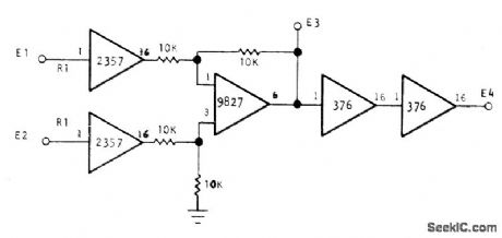
Circuit converts transmission parameter of spectrophotometer to more useful density parameter, which in turn can be converted to exposure parameter. Optical Electronics 2357 opamps at input provide 90-dB dynamic range for DC to 1 kHz or40-dB range for DC to 100 kHz, operating basicallyas current amplifiers. 9827 is used as wideband opamp in unity-gain subtracter configuration. Additional 376 opamps are used only for convening to exposure parameter. Use 1000 ohms for R1 with 10-V full-scale inputs.- Conversion of Transmission to Density and Density to Exposure, Optical Electronics, Tucson, AZ, Application Tip 10133.
(View)
View full Circuit Diagram | Comments | Reading(790)
VOLUME_UNIT_DISPLAY_AND_ALARM_1
Published:2009/7/13 4:39:00 Author:May
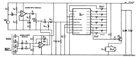
The concept is achieved by using two input modules, namely the sound input circuit and the signal mixer circuit, and selecting between them by means of a switch. The signal is then processed by an integrated circuit (IC3) and associated components, which convert a rising and falling voltage into a rising and falling LED display. The buzzer output module is connected so that when the appropriate LED lights, the buzzer sounds, indicating the excess level warning. (View)
View full Circuit Diagram | Comments | Reading(786)
PHASE_CONTROLLED_DIMMER
Published:2009/7/13 4:39:00 Author:May
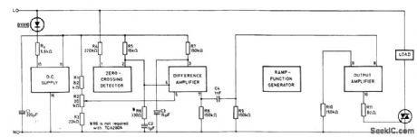
Mullard TCA280A trigger modulels connected to comρare amplitude of ramp waveform with controllable DC voltage in difference amplifier,At point of coincidence, trigger pulse is produced in output amplifier for triggering triac that controls lamp load. Choice of triac depends on load.Values shown for C4 and R9 give 100-μs pulse—''TCA280A Tigger IC for Thyristors and Triacs, ''Mullard, London, 1975,Technical Note19,TP 1490,p 12. (View)
View full Circuit Diagram | Comments | Reading(3060)
CALCULATOR_COUNTS_BY_4s
Published:2009/7/13 4:39:00 Author:May
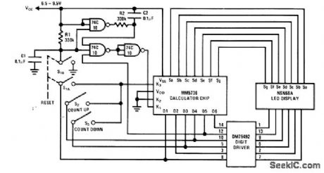
Connection shown for National MM5736 calculator chip counts either up or down by 4s, as might be required for keeping track of inventory in bin when parts are packaged in groups of 4. To count by numbers other than 1, desired number is entered into calculator during manual start operation. When S2 is pushed, counter adds 4 to accumulated total. When S3 is pushed, counter subtracts 4 from accumulated total. Logic ele-ments provide self-starting action of counter. -M. Watts, Calculator Chip Makes a Counter, National Semiconductor, Santa Clara, CA, 1974 AN-112,p5. (View)
View full Circuit Diagram | Comments | Reading(1074)
MULTIPLE_TIMER_FOR_PRINTS
Published:2009/7/13 4:38:00 Author:May
Six independent 2-min timers, each using half of SN7473N IC, are set in sequence by unique input switch as sheets of exposed paper are inserted in developer at about 20-s intervals. When capacity of six prints is reached, Tr12 turns on light to tell operator that no more prints should be inserted until control logic activates alarm signifying 2-min time for first sheet inserted. Audible bleep is repeated as each subsequent sheet reaches its 2-min development time. Article gives all circuits and explains operation in detail. Two-input NAND gates (each 1/4 of SN7400N) and inverters (each1/6 of SN7404N) are used to steer reset pulses. Similar twoinput NAND gates are used to form fully compatible input pulses from input switch control, each having correct level, rise time, and fall time, without contact bounce that might cause spurious starting of several timers simultaneously.-R. G. Wicker, Photographic Development Timer, Wireless World, April 1974, p 87-90. (View)
View full Circuit Diagram | Comments | Reading(953)
CB_CONVERTER
Published:2009/7/13 4:38:00 Author:May
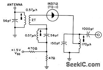
Uses tunnel-diode oscillator.- Transistor Manual, Seventh Edition, General Electric Co,1964, p358. (View)
View full Circuit Diagram | Comments | Reading(937)
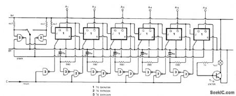
CLEAN_RESET
Published:2009/7/13 4:37:00 Author:May
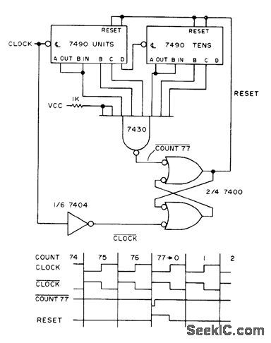
Adding latch consisting of two 7400 NAND gates to reset circuit of divide-by-77 counter guarantees good reset. Reset pulse will always be half a clock period wide. -E. E. Hriv-nak, House Cleaning the Logical Way, 73 Mag-azine, Aug. 1974, p 85-90. (View)
View full Circuit Diagram | Comments | Reading(807)
MOSFET_GATE_DRIVER
Published:2009/7/13 4:37:00 Author:May
This ratiometric 20-kHz voltage-to-frequency converter(VFC) provides superior performance with strain gauges and other ratio-responding transducers,even with noisy, unregulated excitation voltages. Feedback isn’t used to achieve the excellent 4-Hz linearity,so there is very low frequency jitter-period measurements can be used to get several digits of resolution even when operating at a fraction of full scale. An operational synchronizing transistor starts the VFC with zero charge at the beginning of each count Cycle,eliminating the characteristic digit jumping often encountered with VFC designs. Good linearity is attained by making the comparator’s reference voltage vary with the input voltage, which precisely compensates for the finite capacitor reset Lime∶ Period=t1+t2 =t1+(Vcc-Vref)/AVin =[t1AVin+Vcc-Vref)/AVinwhere AVin=ΔV/Δt. If Vref is made to include the amount t1AVin, then the effect of t1 is eliminated∶ Period=[t1AVin+VCC-(t1AVin+Vref)]/AVinThe MPSA-18 is a remarkably high-gain transistor,even at low currents,giving good currentSource linearity down to 0 Hz. In addition,bipolar transistors work well with the low collector voltages encountered In this single-supply,10-V design . Moreover,most single-supply op amps will work in place of the LM10. But the LM10 also has a reference amplifier that could be used to construct a 10-V excitation regulator . The LM311 propagation delay gives a reset pulse width near 400 ns,which gives the transistor time to discharge the capacitor. Also,the 311’s bias current gives a small negative offset that ensures a 0-Hz output for0 V in.
(View)
View full Circuit Diagram | Comments | Reading(1655)
FLASH_TRIGGER
Published:2009/7/13 4:33:00 Author:May
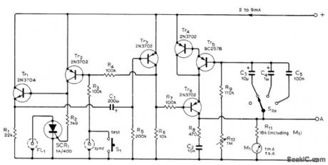
Used in instrument designed to trigger up to five individual flash units at equal increments of time that can rangefrom 11 ms to 11s, as required for such assignments as taking sequence photographs of springboard diver in flight. Transistors Tr1, Tr2, and Tr3 form monostable MVBR that is switched to unstable state by negative pulse applied to base of Tr2 by SCR1 when camera shutter contacts FL1 are closed. Timing circuit Tr4-Tr5-Tr6 provides ramp output at A for feeding voltage-operated switches set to trip at different points of ramp waveform as required for triggering flashes in sequence. Article gives all circuits and setup procedure. Regulated 19.5-V supply is required.-R. Lewis, Multi-Flash Trigger Unit, Wireless World, Nov. 1973, p 529-532. (View)
View full Circuit Diagram | Comments | Reading(856)
2_BIT_BINARY
Published:2009/7/13 4:32:00 Author:May
Sections of RS7473 dual flip-flop are connected to form simple counter that counts to three in binary with LEDs, By adding more flip-flop stages, count can be extended to higher values. If OFF LED represents 0 and ON LED is 1, combinations 00, 01, 10, and 11 rep-resent 0, 1, 2, and 3, respectively. Input is restricted to low audio frequency so LED changes can be readily observed during demonstrations. -F. M. Mims, Integrated Circuit Projects, Vol, 6, Radio Shack, Fort Worth, TX, 1977, p23-32. (View)
View full Circuit Diagram | Comments | Reading(700)
CONSTANT_CURRENT_DIODE_AS_COLLECTOR_LOAD
Published:2009/7/13 4:32:00 Author:May
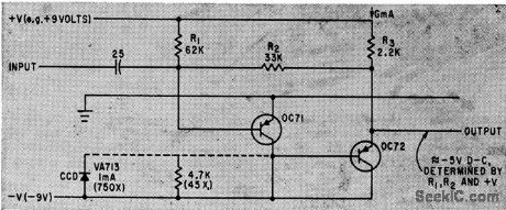
Gain is 45 with 4.7K resistive load, and increases to 750 with CCD as load.Gain-reducing effect of external load paralleling CCD can be eliminated by using emitter.follower to isolate load from collector circuit.-T.K.Hemingway, Applicclfions of the Constant-Current Diode,Electronics, 34:42, p 60-63. (View)
View full Circuit Diagram | Comments | Reading(1395)
BAR_GRAPH_DISPLAY_DRIVER_SCALE_SETTING
Published:2009/7/13 4:31:00 Author:May
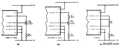
The figure shows ways of varying the reference with the internal generator of the bar-graph driver chip. (a) and (b) show two obtain full scales of 1 V and 0.5 V, respectively. In (c), the reference adjust and internal reference are used to produce 2 V. (View)
View full Circuit Diagram | Comments | Reading(723)
| Pages:179/471 At 20161162163164165166167168169170171172173174175176177178179180Under 20 |
Circuit Categories
power supply circuit
Amplifier Circuit
Basic Circuit
LED and Light Circuit
Sensor Circuit
Signal Processing
Electrical Equipment Circuit
Control Circuit
Remote Control Circuit
A/D-D/A Converter Circuit
Audio Circuit
Measuring and Test Circuit
Communication Circuit
Computer-Related Circuit
555 Circuit
Automotive Circuit
Repairing Circuit