
Index 163
GATED_OSCILLATOR
Published:2009/7/16 1:47:00 Author:Jessie
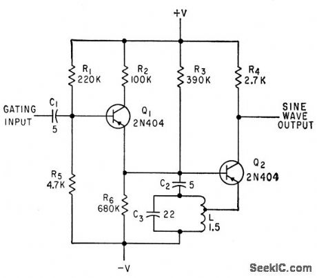
Drives pair of pulse generators for selective calling system.-A. I. Perlin, Selective Calling for Data Link Systems, Electronics, 33:18, p 108-110. (View)
View full Circuit Diagram | Comments | Reading(1468)
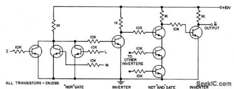
MULTIEMITTER_TRANSISTOR_ALTERNATES_BETWEEN_AND_OR_LOGIC
Published:2009/7/16 1:47:00 Author:Jessie
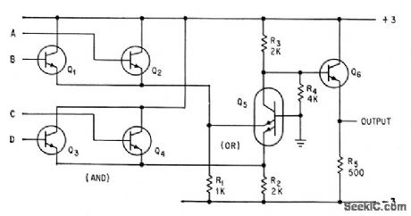
Circuit performs and function first, then or function. For integrated-circuit construction, few isolated lands ore needed.-P. M. Thompson, Logic Principles for Multi-emitter Transistors, Electronics, 36:37, p 25-29. (View)
View full Circuit Diagram | Comments | Reading(557)
EXPONENTIAL_RAMP
Published:2009/7/14 0:34:00 Author:May
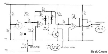
Used in curve tracer in which ramp does not need to be linear. Input romp output UJT Tr1 is Texas Instruments 43 or equivalent, ICs are SN72558P dual opamp or individual SN72741P opamps, and diodes are 1S44 or equivalent. Article gives other circuits and calibration procedure.-L.G. Guthbert, An F.E.T. Curve Tracer, Wireless World, April 1974, p 101-103. (View)
View full Circuit Diagram | Comments | Reading(973)
TANDEM_BRIDGE_FET
Published:2009/7/16 1:46:00 Author:Jessie
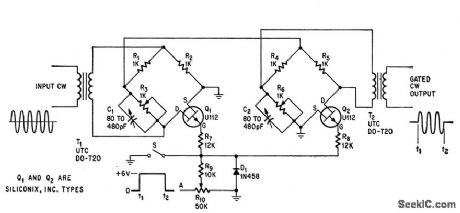
Provides tone bursts from 300-kc c-w input. Signal leakage in off condition is down 60 db.-F. J. Murphree and J. Bealor, FET in Bridge Circuit Gates a 300-KC Signal, Electronics, 38:9, p 60-61. (View)
View full Circuit Diagram | Comments | Reading(692)
DIGITAL_RAMP
Published:2009/7/14 0:33:00 Author:May
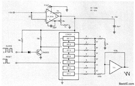
Digiial-to-analog technique using single CD4024A CMOS shift register eliminates temperature and linearity problems normally encountered when using RC circuit to drive VCO of digital ramp. Ramp is generated from 50-kHz clock and stopped by applying reset pulse to counters, Use of stable but variable supply for IC permits adjustment of ramp output amplitude, Ramp itself consists of large number of small steps; if these steps are too large, second CD4024A can be added and clock frequency increased. If response of 741 opamp is not adequate for very steep ramps, use opamp having higher slew rate.-K. Bower, CMOS Linear-Ramp Generator Has Amplitude Control, EDN Magazine, June 20, 1973, p 87. (View)
View full Circuit Diagram | Comments | Reading(2011)
TUNNEL_DIODE_OR_CIRCUIT_AND_ENVELOPE_GENERATOR
Published:2009/7/16 1:45:00 Author:Jessie
Used as part of program pulse generator incorporating ring of four stages, diode-matrixed with ring of three stages to provide twelve-bit words at 30-Mc dock rate.C6 and R2 are a-c terminations for coax from output of ring counter.-W. V. Harrison and R. S. Foote, funnel Diodes Increase Digital-Circuit Switching Speeds, Electronics, 34:32, p 154.-156. (View)
View full Circuit Diagram | Comments | Reading(669)
VOLTAGE_CONTROLLE_D_RAMP
Published:2009/7/14 0:31:00 Author:May
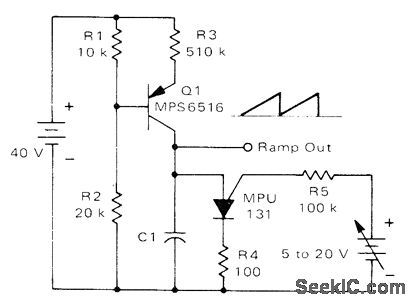
Current source Q1 and C1 together set duration time of ramp. As positive DC voltage at gate of MPU131 is increased, peak point firing voltage of PUT is changed and duration time is increased. With 0.01μF, control voltage change from 5 V to 20 V increases duration time linearly from 2 ms to 7.2 ms.-R. J. Haver and B. C. Shiner, Theory, Characteristics and Applications of the Programmable Unijunction Transistor, Motorola, Phoenix, AZ, 1974, AN-527, p 8. (View)
View full Circuit Diagram | Comments | Reading(821)
LIN_LOG_SWEEP
Published:2009/7/14 0:30:00 Author:May
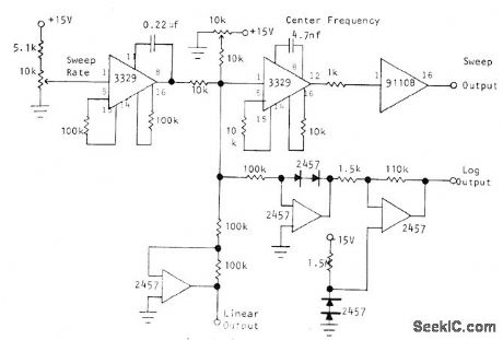
Sweep rate and center frequency are adjustable in versatile sweep generator providing sweep-frequency output and both linear and logarithmic voltages representing output frequency. Optical Electronics 3329 voltage-to-frequency transducer generates sweep voltage at frequency determined by external resistors, capacitor, and input voltage from 10K pot. Sweep waveform is triangular; for sawtooth waveform, change one of 100K timing resistors to 10K. Second 3329 delivers frequency-varying sine wave to 9110B buffer. 10K pot determines center frequency. Stable log f output is obtained with 2457 log module, Frequency and sweep rates can be range-switched from DC to 100 kHz by changing timing capacitor.- Improved Sweep Generator, Optical Electronics, Tucson, AZ, Application Tip 10209. (View)
View full Circuit Diagram | Comments | Reading(2509)
FREQUENCY_SYNTHESIZER_
Published:2009/7/13 23:55:00 Author:May
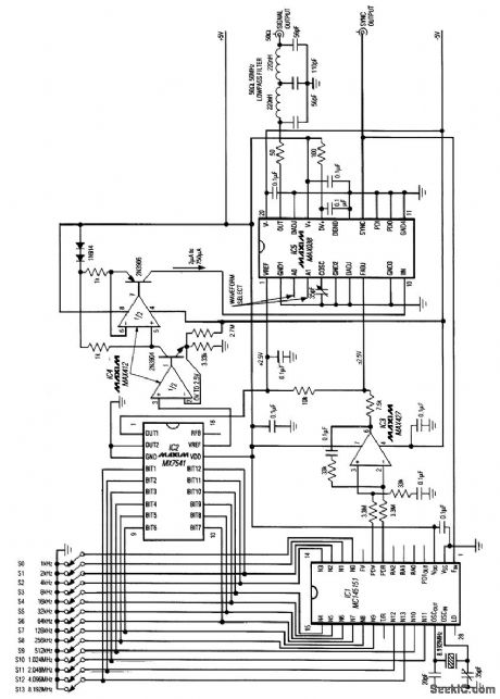
The MAX038 and four other ICs can form a crystal-controlled, digitally programmed frequency synthesizer that produces accurate sine, square, or triangle waves in 1-kHz increments over the range 8 kHz to 16.383 MHz. Each of the 14 manual switches (when open) makes the listed contribution to output frequency: Opening only S0, S1, and S8, for example, produces an output of 259 kHz. The switches generate a 14-bit digital word that is applied in parallel to the D/A converter (IC2) and a ÷N circuit in IC1. IC1 also includes a crystal-controlled oscillator and high-speed phase detector, which form a phase-locked loop with the voltage-controlled oscillator in IC5. The DAC and dual op amp (IC4) produce a 2- to 750-μA current that forces a coarse setting of the IC5 output frequency-sufficient to bring it within capture range of the PLL. This loop, in which the phase detector in IC1 compares IC5's SYNC output with the crystal-oscillator frequency divided by N, produces differential-phase information at PDV and PDR. IC3 then filters and converts this information to a ±2.5-V single-ended signal, which, when summed with an offset and applied to FADJ, forces the signal output frequency to the exact value set by the switches. (View)
View full Circuit Diagram | Comments | Reading(1941)
ZERO_SET_FOR_90_DIODE_MATRIX
Published:2009/7/13 23:49:00 Author:May
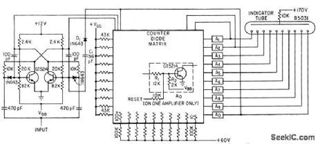
Each pulse input to lip-lop advances counter one position. Single-transistor amplifiers A1-A0 drive glow indicator tube serving as readout. For reset to zero, positive pulse is applied to base of transistor in zero amplifier, to turn its transistor on and turn all other amplifier transistors off.-R.W. Wolfe, Diode Matrix Shrinks Decimal Counter, Electronics.35:13,P50-52 (View)
View full Circuit Diagram | Comments | Reading(640)
SLOT_FILTER
Published:2009/7/16 1:45:00 Author:Jessie
Interval-sensitive gate will detect tone in range from 4,900 to 5,100 cps regardless of other frequencies present.-A. Corbin, Digital Tone Filter with Infinite Rejection Slope, Electronics, 34:5, p 58. (View)
View full Circuit Diagram | Comments | Reading(684)
PUMPED_TUNNEL_DIODE_TRANSISTOR_LOGIC_GATE
Published:2009/7/16 1:43:00 Author:Jessie
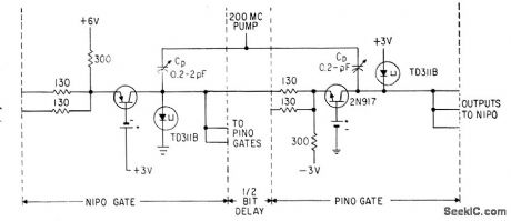
Nipo gate accepts negative inputs and provides positive outputs, while pino gate accepts positive inputs and provides negative outputs. With no inputs, 200-Mc pump or dock has sufficient amplitude to fire nipo stage tunnel-diode on positive half-cycle and pino stage tunnel-diode on negative half-cycle. When input signal is present, pump cannot ire that tunnel diode; this is basic nor gate action, with output pulse only when there is no input.-E. Gottlieb and J. Giorgis, Tunnel-Diode Switching Circuits, Electron'nos, 36:27, p. 26-31. (View)
View full Circuit Diagram | Comments | Reading(751)
NEON_PHOTOCONDUCTOR_IN_LOW_COST_LOW_SPEED_GATE
Published:2009/7/16 1:43:00 Author:Jessie
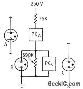
Cadmium selenide or cadmium sulfide photoconductors PC deposited on common substrate are used in pairs with Ne-2H miniature neon indicator lamps to replace electromechanical relays in low-speed digital gate. Firing time of neons is reduced and stabilized by applying 350 V, 60-cps voltage between one neon electrode and adjacent external electrode, to maintain am bient light that gives low level of ionization in lamp.-J. L. Patterson, Will Neon Photo-conductors Replace Relays in Low-Speed Logic?, Electronics, 36:18 p 46-49. (View)
View full Circuit Diagram | Comments | Reading(690)
STEPPING_SWITCH_POSITION_INDICATOR
Published:2009/7/16 1:43:00 Author:Jessie
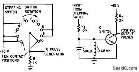
Transistor Q generates positive output pulse when input pulse is applied or removed. To obtain such positive pulses when stepping switch of automatic test set reaches positions 1, 3, 4, 5, 8, and 10, contacts ore connected to -10 V. Transfer for contact 1 to 2 then gives no output pulse, but moving from 2 to 3 removes input pulse and thus gives deisired output pulse. Operation depends on under clamped oscillation in unloaded R-L-C ' circuit, with only one negative oscillation because saturated transistor shunts tuned network.-R. J. Bouchard, Positive. Pulse Gen. orator, Electronics, 37:21, p 74-75. (View)
View full Circuit Diagram | Comments | Reading(785)
UP_OR_DOWN
Published:2009/7/13 23:40:00 Author:May
Scr ring counter shifts up or sown in 3 millisec without missing count. Only conducting stage draws power.-J.G. Peddie, SCR Ring Counter Switches Up or Down. Electronics.38:18.p84-85 (View)
View full Circuit Diagram | Comments | Reading(1108)
BLOCKING_OSCILLATOR_FOR_SHIFT_REGISTER
Published:2009/7/16 1:42:00 Author:Jessie
Used to generate series of ten pulses, 20 nsec wide and spaced 40 nsec apart. Each of the ten blocking oscillator stages Q1 is allowed to overshoot and trigger the following stage through an IC coupling network that provides additional delay.-B. K. Ericksen and J. D. Schmidt, Random Pulse Generator Tests Circuits, Encodes Messages, Electronics, 34:25, p 56-59. (View)
View full Circuit Diagram | Comments | Reading(673)
GATE_OUTPUT_INVERTER
Published:2009/7/16 1:42:00 Author:Jessie
Inverter stages compensate for phase inversion of three parallel-transistor nor gates and three series-transistor not and gates.- Transistor Manual, Seventh, Edition, General Electric Co.,1964, p 177. (View)
View full Circuit Diagram | Comments | Reading(717)
GATE_GENERATOR_FOR_MISSILE_TRACKER
Published:2009/7/16 1:41:00 Author:Jessie
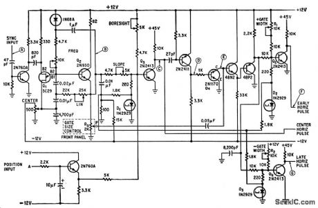
Position of rectangular gate on tv display is controlled by d-c voltage, while size of gate can be adjusted manually without affecting its center position.-J. R. Kruse, Automatic Tv Tracker Keeps Eye on Missiles, Electronics, 34:13, p 82-87. (View)
View full Circuit Diagram | Comments | Reading(763)
ELECTRONIC_PARROT
Published:2009/7/13 23:36:00 Author:May
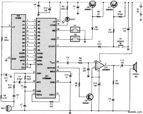
This circuit uses a Holtek HT8656 CMOS LSI chip and an 81256 256K X 1 dynamic RAM chip to form a voice record/playback circuit. The sampling rate is either 16 or 32 kbits per second, which allows 8- or 16-second recording time with the 256K DRAM. A 64K DRAM can be used if shorter times are suitable for your application. Power is via a 9-V battery. (View)
View full Circuit Diagram | Comments | Reading(1116)
25_A_BATTERY_CHARGER
Published:2009/7/13 23:35:00 Author:May
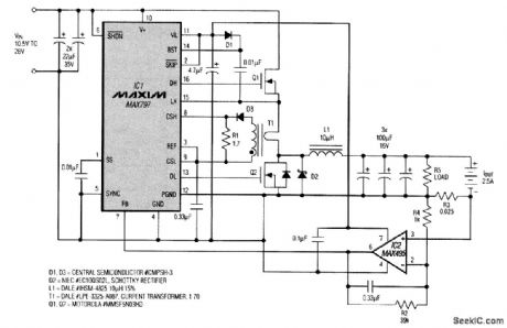
Battery chargers are usually designed without regard for efficiency, but the heat generated by low-efficiency chargers can present a problem. For those applications, the charger shown in the figure delivers 2.5 A with efficiency as high as 96 percent. It can charge a battery of one to six cells while operating from a car battery. IC1 is a buck-mode switching regulator that controls the external power switch, Q1, and the synchronous rectifier. IC1 includes a charge pump for generating the positive gate-drive voltage required by Q1. The battery-charging current develops a voltage across the 25-MΩ resistor (R3) that is amplified by the op amp and presented as positive-voltage feedback to IC1. This feedback enables the chip to maintain the charging current at 2.5 A. While charging, the circuit can also supply current to a separate load, up to a limit set by current-sense transformer T1 and sense resistor R1. T1 improves efficiency by lowering power dissipation in R1. The transformer turns ratio (1:70) routes only 1/70 of the total battery-plus-load current through R1, creating a feed-back voltage that enables IC1 to limit the overall current to a level compatible with the external components. (View)
View full Circuit Diagram | Comments | Reading(1586)
| Pages:163/471 At 20161162163164165166167168169170171172173174175176177178179180Under 20 |
Circuit Categories
power supply circuit
Amplifier Circuit
Basic Circuit
LED and Light Circuit
Sensor Circuit
Signal Processing
Electrical Equipment Circuit
Control Circuit
Remote Control Circuit
A/D-D/A Converter Circuit
Audio Circuit
Measuring and Test Circuit
Communication Circuit
Computer-Related Circuit
555 Circuit
Automotive Circuit
Repairing Circuit