
Index 178
MEASURING_SWITCHING_TIME_OF_IC_GATE
Published:2009/7/16 3:41:00 Author:Jessie
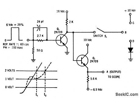
Used for and gates. To measure t1, S1 is opened, input pulse of Q1 is adjusted to give Q1 output fall time of 3 nsec/v slope for 2.5 v, and S1 is closed to measure t2.-Integrctted Circuits, FEE, 12:3, p 78. (View)
View full Circuit Diagram | Comments | Reading(664)
EMITTER_COUPLED_TRANSISTOR_AND_GATE
Published:2009/7/16 3:41:00 Author:Jessie
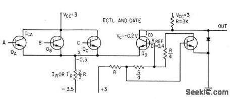
Design gives manufacturing simplicity for integrated circuits without current hogging, but requires two power supplies. QD will con duct and QA QB, and QC will be off when any of input A, B, or C are below 0.2V.-A. E. Skoures, Choosing Logic for Microelectronics, Electronics, 36:40, p 23-26. (View)
View full Circuit Diagram | Comments | Reading(780)
BASIC_RCTL_LOGIC
Published:2009/7/16 3:40:00 Author:Jessie
Transistors used provide ultrahigh switching speed for computers and have low stored charge along with gain-bandwidth product above 300 Mc. Circuit can readily be adapted as flip-flop, nor circuit, and Schmitt trigger.-W. D. Roehr, For Computers... Basic RCTL Circuits, Motorola Application Note AN-129, Nov. 1965. (View)
View full Circuit Diagram | Comments | Reading(836)
TWO_INPUT_PINO_NOR_GATE
Published:2009/7/16 3:40:00 Author:Jessie
Pumped solid-state logic for uhf shift register using positive input-negative output gate gives 2-gc rate.-Tunnel Diode-Transistor Provides Fast Logic, Electronics, 35:11, p 72. (View)
View full Circuit Diagram | Comments | Reading(617)
2_SEC_TO_10_MIN_TIMER
Published:2009/7/16 3:39:00 Author:Jessie
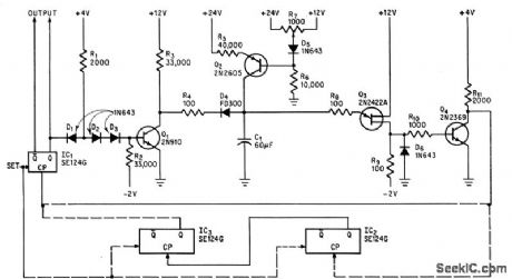


Number of monolithic diode-transistor logic circuits determines range of time delay provided by potentiometer R7. For shorter delays, one or both of integrated circuits connected with broken lines may be eliminated.-A. A. Lampell, Off-the-Shelf Integrated Circuits for Versatile and Accurate Timer, Electronics, 38:25, p 70-73. (View)
View full Circuit Diagram | Comments | Reading(783)
2_AND_4_INPUT_PULSE_NOR_GATE
Published:2009/7/16 3:39:00 Author:Jessie
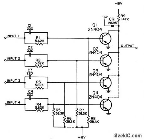
Circuit is special-purpose nor gate for computer, control, and communication equipment. Used for the and operation when a general-purpose nor gate would be unsatisfactory because of possible spurious pulses in output.-NBS, Handbook Preferred Circuits Navy Aeronautical Electronic Equipment, Vol. II, Semiconductor Device Circuits, PSC 8 (originally PC 211), p 8-2. (View)
View full Circuit Diagram | Comments | Reading(772)
DRIVERS_FOR_SHIFT_REGISTER
Published:2009/7/16 3:37:00 Author:Jessie
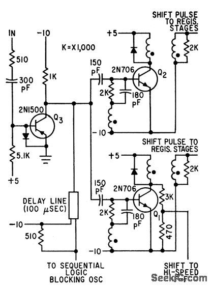
Inverter Q3 pulses 300-ma drivers Q1 and Q2 and feeds 100-nsec delay line that provides time for shift register stages to reach final values in new stale.-B. K. Ericksen and J. D. Schmidt, Random Pulse Generator Tests Circuits, Encodes Messages, Electronics, 34:25, p 56-59. (View)
View full Circuit Diagram | Comments | Reading(664)
IMPROVED_DARLINGTON
Published:2009/7/16 3:37:00 Author:Jessie
Separate collector circuit for, third Transistor of Darlington configuration prevents refection of high capacitance back to input, thereby dissipating Miller effect.-Y. Tarui, Japan Seeks Its Own Route to Improved IC Techniques, Electronics, 38:25, p 90-98. (View)
View full Circuit Diagram | Comments | Reading(726)
DUAL_4_INPUT_GATE
Published:2009/7/16 3:37:00 Author:Jessie
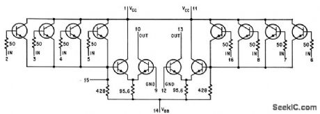
Each 4-input section uses 4-transistor chip for hybrid microelectronic construction.-J. G. Curtis, Crossbred Technology Automates Production of Hybrid Microcircuits, Electronics, 38:13, p 66-73. (View)
View full Circuit Diagram | Comments | Reading(725)
ASTABLE_MVBR
Published:2009/7/16 3:36:00 Author:Jessie

Stress-sensitive RC103 integrated circuit shifts free-running frequency from 500 kc to 1 Mc when 7 grams of force is applied to one transistor.-R. C. Wonson, Stress- Sensitive Integrated Circuits, Electronics, 38:14, p 81-84. (View)
View full Circuit Diagram | Comments | Reading(696)
DIODE_COUPLED_NAND_NOR_GATE
Published:2009/7/16 3:36:00 Author:Jessie
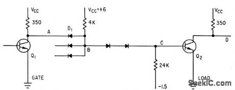
Designed for integrated circuits, arrangement gives unlimited fan-in and high immunity to noise, with 1.7 v logic swing.-A. E. Skoures, Choosing Logic for Microelectronics, Electronics, 36:40, p 23-26. (View)
View full Circuit Diagram | Comments | Reading(708)
MONOSTABLE_MVBR
Published:2009/7/16 3:36:00 Author:Jessie
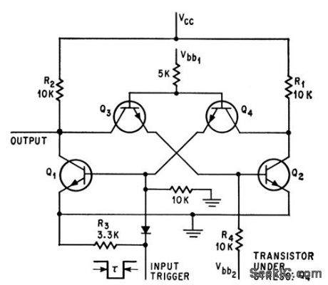
Pulse width of stress-sensitive RC103 integrated circuit is reduced from 1.5 to 1.0 microsec when 7 grams of force is applied to one transistor-R. C. Wonson, Stress-Sensitive Integrated Circuits, Electronics, 38:14, p 81-84. (View)
View full Circuit Diagram | Comments | Reading(763)
COMPLEMENTARY_RDTL_NOR
Published:2009/7/16 3:35:00 Author:Jessie
Alternately provides 500-na base current to pnp and npn transistors, thereby using transistor rise time at both edges of switching pulse to eliminate R-C time constant fall times of output wave form. Design reduces power drain and speeds up rise and fall times by factor of 15.-R. A. Tietsch, Complementary Microwatt Logic Circuits, EEE, 11:8, p 51-52. (View)
View full Circuit Diagram | Comments | Reading(746)
RCTL_NAND_NOR_GATE
Published:2009/7/16 3:34:00 Author:Jessie
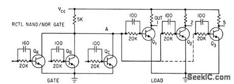
Resistors and capacitors in base circuits permit higher fan-out and give logic swing of 2v for high noise rejection in integrated-circuit logic.-A. E, Skoures, Choosing Logic for Microelectronics, Electronics, 36:40, p 23-26. (View)
View full Circuit Diagram | Comments | Reading(693)
1_WATT_AUDIO_AMP
Published:2009/7/16 3:34:00 Author:Jessie
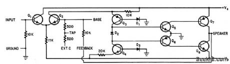
Negative d-c and ac feedback is applied to one side of differential input stage and signal to other side. With balanced power supplies, d-c output is at ground, permitting direct drive of speaker without lage d-e decoupling capacitor in MC1524 integrated circuit.-R. Hirschfeld, IC's Improve Differential Amplifiers-and Vice Versa, Electronics, 38:16, p 75-79. (View)
View full Circuit Diagram | Comments | Reading(890)
SINGLE_CRYSTAL_FOR_46_TO_420_MHz
Published:2009/7/16 3:33:00 Author:Jessie
Covers all VHF amateur bands by using mixer-generated harmonics of 66-MHz crystal oscillator frequency for mixing action. IF can be tuned with any communication receiver. Fundamental is used directly, third harmonic of 138 MHz serves for 2 meters, fifth of 230 MHz for 220-MHz band, and ninth of 414 MHz for 420-MHz band. Q1-Q3 are broadband RF preamp. Y1 is plated overtone crystal oscillating at 46 MHz in series-resonant mode. Q5 and Q6 form differential-amplifier oscillator, and Q4 is mixer driver. No tuning is required in converter, but external tuning is required to prevent device from working on all bands at once. All transistors are part of RCA CA3049T IC, for which pin numbers are circled. L1 is 72 inches of No. 30 enamel, doubled and twisted 1 turn per inch and wound on 1-meg-ohm 1/2-W resistor to form quarter-wave trans-mission line. -S. Smith, Four-Band VHF Receiving Converter, Ham Radio, Oct. 1976, p 64-66. (View)
View full Circuit Diagram | Comments | Reading(1011)
ALL_CMOS_RECEIVER
Published:2009/7/16 3:32:00 Author:Jessie
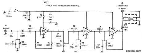
Uses CD4007A IC, having complementary ρair of opamps and inverter, to provide all circuits for AM broadcast radio capable of driving headphones or 8-ohm loudspeaker, Selectivity is provided by single tuned circuit and can be improved by optimizing value of C1 to adjust antenna loading. Tune with C3, adjusting L1 if necessary to get stations at low end of band. - C. Green, Easy-to-Build CMOS Radio Receiver, Modern Electronics, Sept. 1978, p 4-41, 46, and 59. (View)
View full Circuit Diagram | Comments | Reading(1035)
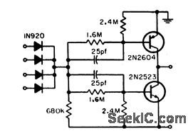
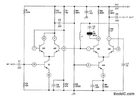
HARMONIC_MIXER
Published:2009/7/16 3:32:00 Author:Jessie
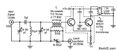
Two-transistor integrated circuit is used in nonlinear mode for converting 120 Mc to 10.7 Mc with conversion of 29.4 db, noise figure of 11 db, and sensitivity of -105 dbm. Bandwidth, including i-f stages that follow mixer, is about 500 kc.-J. E. Thompson, An Integrated Harmonic Mixer, Motorola Application Note AN-154, December, 1965. (View)
View full Circuit Diagram | Comments | Reading(1635)
LINEAR_IC_TESTER
Published:2009/7/16 3:30:00 Author:Jessie
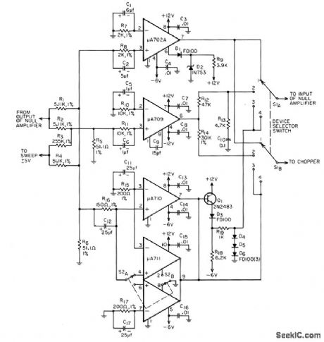
Basic lab tester circuit displays transfer function, offset voltage, gain, linearity, and output voltage swing on single scope trace. High-gain null opera tional amplifier (such as Fairchild 709 IC) is used in feedback loop around linear integrated-circuit amplifier under test, to hold output of amplifier under test at zero by adjusting its d-c input voltage to equal the offset. Chopper on vertical scope inputs allows simultaneous display of offset voltage and transfer function, by switching in synchronism with horizontal sweep. Separate TO-5 socket is provided for each type of integrated circuit to be tested.-J. N. Giles, How to Measure Linear-IC Performance, EEE, 14:8, p 62-68 and 161. (View)
View full Circuit Diagram | Comments | Reading(1884)
80_METER_TUNER
Published:2009/7/16 3:27:00 Author:Jessie
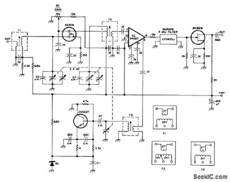
RF stage uses dual-gate N-channel enhancement-mode Signetics SD304 operating with positive bias. With 0-6V applied to gate 2, AGC range is about 40 dB, but circuit shown uses manual BF gain control. Extra stage of IF overcomes insertion loss of 3-kHz ceramic ladder filter. SG3402T IC is used in mixer; remove pin 6. Transformers T1, T2, and T3 are wound on standard 3/8-in IF forms.-R. Megirian, Design Ideas for Miniature Communications Receivers, Ham Radio, April 1976, p 18-25. (View)
View full Circuit Diagram | Comments | Reading(1149)
| Pages:178/471 At 20161162163164165166167168169170171172173174175176177178179180Under 20 |
Circuit Categories
power supply circuit
Amplifier Circuit
Basic Circuit
LED and Light Circuit
Sensor Circuit
Signal Processing
Electrical Equipment Circuit
Control Circuit
Remote Control Circuit
A/D-D/A Converter Circuit
Audio Circuit
Measuring and Test Circuit
Communication Circuit
Computer-Related Circuit
555 Circuit
Automotive Circuit
Repairing Circuit