
Index 166
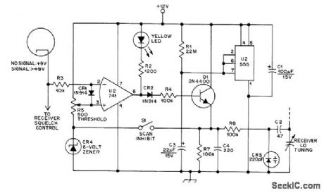
NONCUTOFF_MONOSTABLE
Published:2009/7/15 23:35:00 Author:Jessie
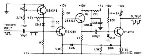
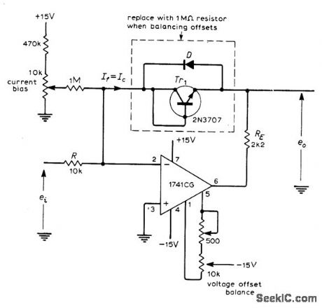
Optimum operating conditions are achieved by keeping amplifiers connected to current sources continuously. With constant input voltage, triggering makes threshold level shift. Diodes in feedback loop improve switching speed. -H. Inose, Y. Yoshida, and H. Tada, Noncutoff Circuits Improve Trigger Switching, Electronics, 35:30, p. 36-39. (View)
View full Circuit Diagram | Comments | Reading(720)
STEERING_FOR_REVERSIBLE_DECADE_COUNTER
Published:2009/7/13 23:03:00 Author:May
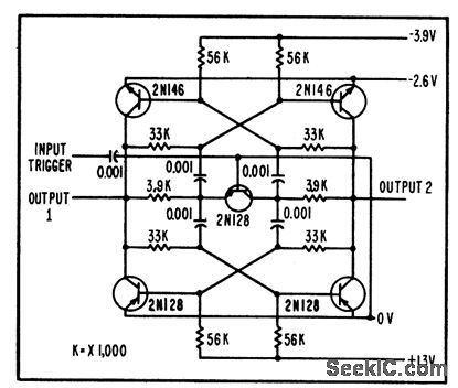
Consists of four R-C coupled complementary saturated flip-flops Q1-Q8. Symmetrical npn steering fransistors Q9 through Q16, coupled between collectors of flip-flops, are used as trigger current amplifiers and for steering when counting up or down.-R..D. Carlson, Steering Circuits Control Reversible Counters, Electronics, 33:1, p 86-88. (View)
View full Circuit Diagram | Comments | Reading(745)
CARBON_MIKE_FOR_MOBILE_SERVICE
Published:2009/7/13 22:53:00 Author:May
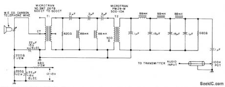
Filter enhances desirable characteristics of ordinary carbon mike taken from telephone, for use with mobile transceiver. Required excitation voltage of 3.5 V for mike is reduced from 12 V of car battery by resistor network having hash filter to keep alternator whine out of audio system. Output of 0.25 mV from mike-filter combination is reduced by 100K pot to value needed for transmitter.-S. Olberg, The Carbon Marvel, 73Mag-azine, April1977, p 120. (View)
View full Circuit Diagram | Comments | Reading(986)
TEMPERATURE_COMPENSATED_LOG_CONVERTER
Published:2009/7/13 22:50:00 Author:May
Two opamps and two logging transistors give output proportional to logarithm of input with high degree of temperature compensation. Article gives design equations and application instructions. Circuit is for positive inputs; for negative inputs, use PNP transistors such as 2N4058 in place of those shown.-G. B Clayton, Experiments with Operational Amplifiers, Wireless World, Jan. 1973, p 33-35. (View)
View full Circuit Diagram | Comments | Reading(976)
SINE_WAVE_DOUBLER
Published:2009/7/13 22:50:00 Author:May

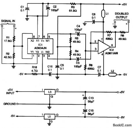
This circuit uses a four-quadrant multiplier by Analog Devices to perform frequency doubling on a sine-wave input signal. By applying a sine wave to both x and y inputs, the multiplier muitiplies the sine wave by itself, resulting in a sine-squared waveform. This waveform is equivalent to a dc level and a cosine component at twice the frequency and half the original amplitude, i.e., sin2x(1-cos 2x)/2-3 dB bandwidth is typically 30 MHz. (View)
View full Circuit Diagram | Comments | Reading(1745)
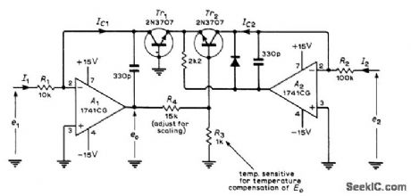
TEMPERATURE_COMPENSATED_ANTILOG_CONVERTER
Published:2009/7/13 22:44:00 Author:May
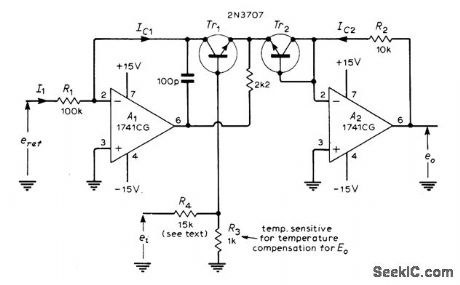
Circuit provides antilog conversion with high degree of temperature compensation. Article gives design equations and application instructions. Circuit is for positive inputs; for negative inputs, use PNP transistors such as 2N4058 in place of those shown. Adjust value of R4 to make output of opamp A2 exactly 10 times input voltage ei when input is -1 V.-G. B. Clayton, Experiments with Operational Amplifiers, Wireless World, Jan, 1973, p 33-35. (View)
View full Circuit Diagram | Comments | Reading(1742)
SHAFT_ENCODER
Published:2009/7/13 22:44:00 Author:May
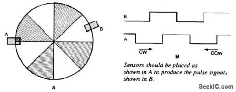
The electro-optical shaft encoder is a combination of encoding disk, photosensors, and counters. The encoding disk and photosensors generate a pulse train that can be counted to determine rate. The disk's direction of rotation can be sensed and used to determine count direction (for example, count up for clockwise and count down for counterclockwise). The disk need not be a precision part; it can be tytade from clear plastic with dark sections or lines painted on it. The number of lines on the disk determines how many pulses are generated per revolution. If two photosensors are used, two signals in quadrature are generated; from those, the direction can be sensed. A simple encoding disk is shown in A; note the alternating transparent and opaque sections. A pair of electro-optical photosensors are positioned (as shown) so that when one is centered over a section, the other is positioned over a transition. As the disk is rotated, each photosensor will be alternately illuminated and obscured and will produce outputs (as shown). A clockwise rotation is indicated when there is a positive transition (from dark section to light section) at sensor B while sensor A is low (obscured by a dark section), a positive transition at A while B is high (over a light section), a negative transition of B (going from light to dark) while A is high, and so forth. A counterclockwise rotation is indicated when there is a positive transition of B when A is high, a negative transition of A when B is high, etc. (View)
View full Circuit Diagram | Comments | Reading(3110)
SHAFT_ENCODER_PULSE_GENERATING_CIRCUIT
Published:2009/7/13 22:42:00 Author:May
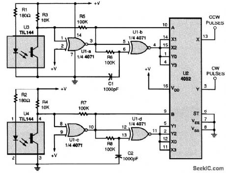
This circuit produces one output pulse for every transition of the photosensor output or four pulses for every section or line pair. The exclusive-NOR gates U1-b and U1-c produce a pulse on every transition, and U2, a dual four-channel data selector, decodes them into up pulses or down pulses. The number of sections or lines that can be accommodated on a disk is determined by its diameter and the width of the sections. As an example, if the sections are made approximately 0.125 wide, 25 section pairs can put on a 2 diameter disk and 100 pulses will be generated with every revolution of the disk. The only limiting factor is that the sections must be wider than the photosensor's aperture at the point they pass in front of it, The alignment of the photosensor assembly is not critical. The only concern is that one sensor be over a light area while the other sensor is at a transition from light to dark or dark to light. 1Vro sections of U1, U1-a and U1-c, act as buffers and waveshapers for the outputs of the sensor, while U1-b and U1-d generate a pulse at each transistor of the sensor's output. The 100-k Ω resistors between the output and the input of U1-a and U1-c provide positive feedback to speed up the rise and fall times and also generate hysteresis to eliminate noise during the transitions. The pulses produced by U1-b and U1-d at the transitions are the result of the delay produced by the RC circuits located at one input of each gate. For example, U1-b pin 5 follows the transition immediately, whereas pin 6 follows slowly. With the values shown, the two inputs are different for about 100 μs after every transition. While the inputs are different, the output is low. Therefore, U1-b generates a negative pulse for every transition of sensor U3 and U1-d generates a negative pulse for every transition of U4. The states of U3 and U4 determine whether the pulse is sent to the X output of the data selector (U2, pin 13) to indicate a CCW pulse or to the Y output (pin 3) to indicate a CW pulse. (View)
View full Circuit Diagram | Comments | Reading(2813)
ANALOG_DIVIDER
Published:2009/7/13 22:39:00 Author:May
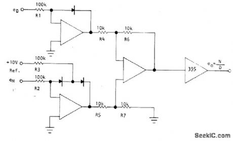
Optical Electronics 2457 logarithmic module containing two pair of bipolar log elements and three opamps drives single 395 opamp to provide analog division function with high accuracy and wide dynamic range. Input resistors set full-scale input voltage. R3 determines AC accuracy. Connect inputs together fot drive with signal varying between 100 mV and 10 V (1% to 100%of full scale), and adjust R3 for straight-ine output at1 V. For negative inputs, reverse diode connections and make reference voltage negative.- Accurate Logarithmic Analog Divider, Optical Electronics, Tucson, AZ, Application Tip 10213. (View)
View full Circuit Diagram | Comments | Reading(2347)
OPTOISOLATOR_DRIVE
Published:2009/7/13 22:35:00 Author:May
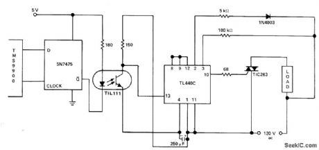
TL440 zero-crossover switch uses pulsed gate drive. Switch supplies phase-locked driving pulses during zero-voltage crossover period, to minimize electromagnetic interference generated during turn-on of triac. Works well with resistive loads, but inductive loads can create phase shift that affects firing time of triac.- Thyristor Gating for μP Applications, Texas Instruments, Dallas, TX,1977,CA-191,p 6. (View)
View full Circuit Diagram | Comments | Reading(2186)
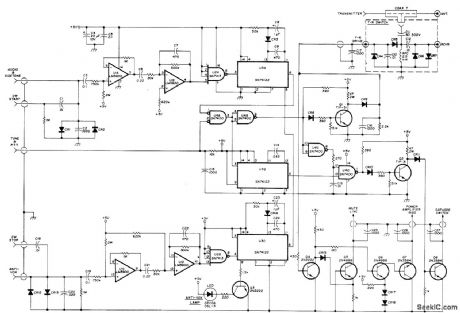
SEISMIC_RADIO_BEACONRF_POWER_AMPLIFIER
Published:2009/7/13 22:32:00 Author:May
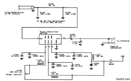
This RF power amplifier operates at 432 MHz and was used as a power amplifier for a small transmitter used in an amateur radio beacon that also has seismic monitoring capability. (View)
View full Circuit Diagram | Comments | Reading(1009)
WARM_UP_DRIFT_COMPENSATOR
Published:2009/7/13 22:30:00 Author:May
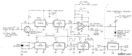
Warm-up drift of transceiver VFO is automatically corrected by using binary counter U1 to count oscillator frequency for interval of about 3.81 Hz determined by 1-MHz reference crystal oscillator and divider chain U4-U5. Switches labeled UP and D0WN are used to bring output of integrator R3-C3 into range manually after circuit switch-on. –K. Spaargaren, Drift-Correction Circuit for Free-Running Oscillators, Ham Radio, Dec, 1977,, p 45-47. (View)
View full Circuit Diagram | Comments | Reading(783)
SEISMIC_RADIO_BEACON(TIMER_AND_SWITCHING)
Published:2009/7/13 22:30:00 Author:May

This timing circuit is fed by a threshold circuit that is actuated by selsmlc activity, as picked up by a geophone The timing is adjustable and controls a 123-Hz PL tone that feeds a transmitter (View)
View full Circuit Diagram | Comments | Reading(647)
HALF_WAVE_FEEDBACK
Published:2009/7/13 22:27:00 Author:May
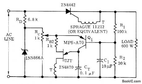
Provides phase control of power to resistive load in applications where average load voltage is desired feedback variable. RC network R1-R2-C1 averages load voltage so it can be compared with set point on Rc by Q1.-D. A. Zinder, Unijunction Trigger Circuits for Gated Thyristors, Motorola, Phoenix, AZ, 1974, AN-413,p 4.
(View)
View full Circuit Diagram | Comments | Reading(629)
BASIC_LOG_CONVERTER
Published:2009/7/13 22:27:00 Author:May
Suitable for positive input voltages. Negative feedback is applied to opamp through diode-connected transistor, with additional diode D protecting transistor from excessive inverse voltage caused by wrong input polarity. For negative inputs, reverse transistor and diode connections. Article gives design equations and application procedures.-G. B. Clayton, Experiments with Operational Amplifiers, Wireless World, Jan. 1973, p 33-35. (View)
View full Circuit Diagram | Comments | Reading(833)
SEISMIC_RADIO_BEACON(THRESHOLD_CIRCUIT)
Published:2009/7/13 22:27:00 Author:May
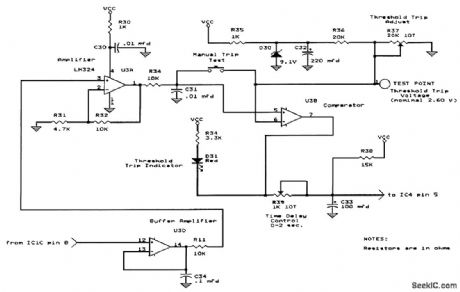
This threshold circuit is fed by a geophone amplifier and is actuated by seismic activity, as picked up by a geophone. The threshold is adjustable. (View)
View full Circuit Diagram | Comments | Reading(1782)
SYLLABIT_VOX
Published:2009/7/13 22:26:00 Author:May
Provides instantaneous radiotelephone speech communication without conventional V0X relays. Switching transistors eliminate contact-bounce problems of relays. Designed for use with Drake T-4XB and R-4B transmitter and receiver. Also gives true breakin CW keying. Since only words and syllables of words go on air, there are no VOX RF transients and no extraneous local noise. Operating bias for final amplifier is applied only during transmission; at other times, final amplifier tubes are completely cut off. Diodes CR4-CR7, CR9, and CR11 are 1N4004 or equivalent. All other diodes are 1N914 or equivalent. RF choke is 2.5 mH rated 100 mA. Article describes operation in detail and gives installation and setup procedures.-R. W. Hitchcock, Syllabic V0X System for Drake Equipment, Ham Radio, Aug. 1976, p 24-29. (View)
View full Circuit Diagram | Comments | Reading(1051)
900_W_FULL_WAVE
Published:2009/7/13 22:24:00 Author:May
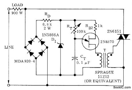
Combination of bridge rectifier, pulse transformer, and triac allows look pot RT to control power to resistive load on both positive and negative half-cycles,Triac is triggered through transformer by 2N4870 UJT,-D.A. Zinder,″Unijunction Trigger Circuits for Gated Thyristors,”Motorola, Phoenix, AZ,1974,AN-413,p 3. (View)
View full Circuit Diagram | Comments | Reading(3734)
5_555_MHz_VFO
Published:2009/7/13 22:24:00 Author:May
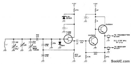
Controls both receiver and transmitter of low-power transceiver for 20 meter amateur band. L1 is 3.5 μH wound on 6mm ceramic form without tuning slug. Number of turns is adjusted to obtain exact inductance. JFET can also be 2N4416 or Motorola MPFl02. VFO is buffered with single-stage feedback amplifier using pair of 2N3904 transistors (transistor type is not critical). Article also gives other circuits of transceiver.-W. Hayward, Low-Power Single-Band CW Transceiver, Ham Radio, Nov. 1974, p 8-17.
(View)
View full Circuit Diagram | Comments | Reading(2636)
300_mA_STEP_DOWN_BATTERY_FOUR_CELL_NiCd_CHARGER
Published:2009/7/13 22:23:00 Author:May
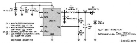
Low-current battery-charger circuits are required in hand-held products such as palmtop, pen-based, and fingertip computers. The charging circuitry for these applications must use surface-mount components and consume minimal board space. The LTC1174 circuit shown provides both of these features. The LTC1174 is a current-mode, step-down switching regulator with a low-loss internal P-channel MOSFET power switch. In this circuit, the peak switch current is programmed to 600 mA. The average charging current is determined by the choice of inductor value and the actual battery voltage, according to the equation. The voltage feedback resistor network is set for an output voltage of 7 Y. NiCd cells have a nominal voltage of 1.2 V, a discharged voltage of 0.9 V, and a fully charged voltage of 1.5 V. A four-cell NiCd pack's voltage will range from 3.6 to 6 V, depending upon its state of charge. When it is attached to the charger, it will pull the output voltage below 7 V and place the LTC1174 into current-limited operation at about 300 mA with the 50-μH inductor shown. Diode D2 prevents the batteries from discharging through the divider network when the charger is shut down by bringing the SHUTDOWN pin low. Less than 10 μA of current is drawn from the sup-ply when the charger is shut down.
(View)
View full Circuit Diagram | Comments | Reading(728)
| Pages:166/471 At 20161162163164165166167168169170171172173174175176177178179180Under 20 |
Circuit Categories
power supply circuit
Amplifier Circuit
Basic Circuit
LED and Light Circuit
Sensor Circuit
Signal Processing
Electrical Equipment Circuit
Control Circuit
Remote Control Circuit
A/D-D/A Converter Circuit
Audio Circuit
Measuring and Test Circuit
Communication Circuit
Computer-Related Circuit
555 Circuit
Automotive Circuit
Repairing Circuit