
Index 173
CAPACITORLESS_NOTCH_FILTER
Published:2009/7/13 10:29:00 Author:May
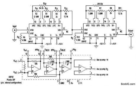
The notch frequency for the filter is set by fnotch+[(ALP/AHP)×(RZ2/RZ1)]×f0where ALP and AHP are the gain from input to low-pass output at f=0 Hz,and the gain from input to high-pass output at f≤f0,respectively. Typically ((ALP/AHP)×(RZ2/RZ1)=1;therefore,fnotch=f0,and is gtven by f0=1/(2π)(RFC)where RF=RF1=RF2, and C=C1=C2. The -3-dB bandwidth is determined by the following relation∶BW-3dB=fnotch/Q, where BW-3dB=fH-fL. The Q of the filter affects the passband gainc(which should be adjusted to unity) and is related to the ratio of the resistances RZ3 to RZ1 and RZ3 to RZ2. In other words,Q=(RZ3/RZ1)=(RZ3/RZ2). Q also is related to RQ by the follOwing relation∶RQ=(25 kΩ/Q-1). (View)
View full Circuit Diagram | Comments | Reading(1076)
INFRARED_HOT_ENGINE_DETECTOR
Published:2009/7/16 3:16:00 Author:Jessie
Output relay resets parking meter to zero when lead sulfide detector senses heat of engine when parked car is started.-W. E. Osborne, Farewell To Free Time On City Parking Meters, Electronics, 37:32, p 72-74. (View)
View full Circuit Diagram | Comments | Reading(726)
NOTCH_FILTER_CIRCUIT
Published:2009/7/13 10:17:00 Author:May
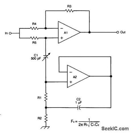
This circuit is basically a noninverting amplifier with positive feedback. The negative feedback path is set to unity by a direct connection between the output terminal of the operational amplifier and the inverting (-) input. A frequency-selective RC network connects the output to the noninverting (+) input, providing some positive feedback. The center frequency is FC=1/2πR1(C1C2)1/2where FC is the center frequency in hertz, R1 is in ohms, and C1 and C2 are in farads. (View)
View full Circuit Diagram | Comments | Reading(1048)
ACTIVE_FILTER_
Published:2009/7/13 10:11:00 Author:May
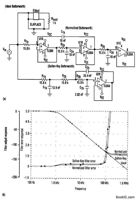
Equal-value components can be quite an advantage in filter designs when the total costs associated with the procurement, stocking, and assembly of the filter are considered. For instance, the Butterworth active third-order low-pass filter (middle) uses equal-value resistors and capacitors. This feature normalizes the filter's 3-dB corner frequency to 1/RC (in radians) for both low-pass and high-pass designs. The graphs in (b) are plots of the ideal, normalized, and Sallen-Key low-pass filter frequency-domain magnitude and error responses. Note how both the normalized and Sallen-Key filters follow the ideal response well into the stopband. The error plots were created by plotting the difference between the real and ideal filter responses. The plots indicate that the normalized filter achieves performance results that are equal to those of the Sallen-Key low-pass filter. (View)
View full Circuit Diagram | Comments | Reading(938)
1_MHz_OR_500_kHz_ELLIPTIC_LP_FILTER
Published:2009/7/13 10:07:00 Author:May
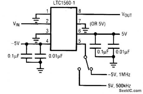
This filter uses a Linear Technology P/N LTC1560-1 to implement a switchable LP filter. (View)
View full Circuit Diagram | Comments | Reading(723)
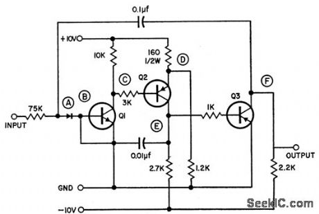
SW_RECEIVER_CW_FILTER
Published:2009/7/13 10:05:00 Author:May
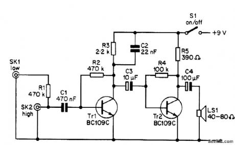
The CW filter is connected between the headphone or loudspeaker socket or terminal strip of your receiver and either the headphones or an external loudspeaker. The output of the receiver should have an intpedance of 8Ω or more. As the circuit provides unity gain at pass frequencies and a low-impedance output, there should be no problems with mismatching when the filter is in use. The frequency response of the circuit peaks at approximately 800 Hz, and the -6-dB bandwidth is about 300 Hz or so. The 0-dB points occur at about 350 Hz and 2 kHz. This is sufficient to normally give a substantial reduction in adjacent-channel interference, but the response is not so narrow and peaky that using the receiver with the filter in the circuit becomes difficult, as the wanted signal tends to drift out of the passband and become lost. (View)
View full Circuit Diagram | Comments | Reading(1096)
INFRARED_POWER_MONITOR
Published:2009/7/16 3:15:00 Author:Jessie
Output of infrared signal generator is monitored by two-thermistor bolometer, low-noise nuvistor preamp, and synchronous detector driving multirange meter, all operating from two highly regulated power supplies.-A. Glaser, Signal Generator for Infrared Region, Electronics, 35:8, p 40-43. (View)
View full Circuit Diagram | Comments | Reading(660)
HIGH_PASS_LOW_PASS_FILTER
Published:2009/7/13 10:03:00 Author:May
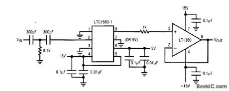
This filter uses a Linear Technology P/N LTC1560-1 and an LT1360 to implement a high-pass/low-pass filter. (View)
View full Circuit Diagram | Comments | Reading(893)
AMATEUR_TRANSMITTER_ABSORPTIVE_FILTER
Published:2009/7/13 10:00:00 Author:May
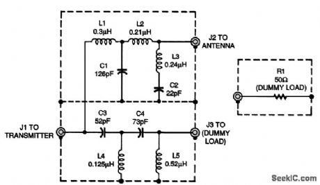
This filter diverts harmonic energy above 30 MHz to a dummy load and dissipates it as heat instead of reflecting it back to the transmitter. The absorptive filter is based on the classic design by Weinreich and Carroll from 1968. The high-pass and low-pass sections are shielded from each other (even though they are in the same shielded box) to prevent interaction. If you want to try building this filter, wind the coils on high-powered toroids. Alternatively, you could wind an air-core coil using the nomograms in The ARRL Handbook for Radio Amateurs. (View)
View full Circuit Diagram | Comments | Reading(753)
PEAKING_FILTER_CIRCUIT
Published:2009/7/13 9:54:00 Author:May
This circuit is basically a noninverting amplifier with positive feedback. The negative feedback is to unity by a direct connection between the output terminal of the operational amplifier and the inverting (-) input. A frequency-selective RC network connects the output to the noninverting (+) input, providing some positive feedback. The center frequency is FC=1/2πR1(C1C2)1/2where FC is the center frequency in hertz, R1 is in ohms, and C1 and C2 are in farads. (View)
View full Circuit Diagram | Comments | Reading(998)
IR_WIDTH_GAGE_AMPLIFIER
Published:2009/7/16 3:11:00 Author:Jessie
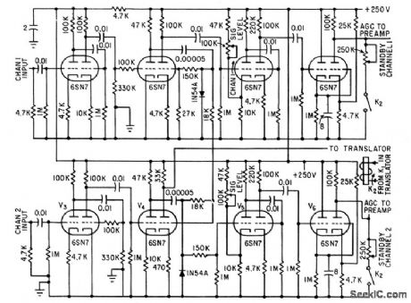
Amplifies signals from two amplifiers, and combines them at second, triode of V4 for translator.Signal here consists of positive-going pulse from channel 1 and negative-going pulse from channel 2, with distance between pulses indicating strip width.-F. J. Danks, Infrared Gage Measures Hot Steel Strip Width, Electronics, 33:43, p 65-67. (View)
View full Circuit Diagram | Comments | Reading(661)
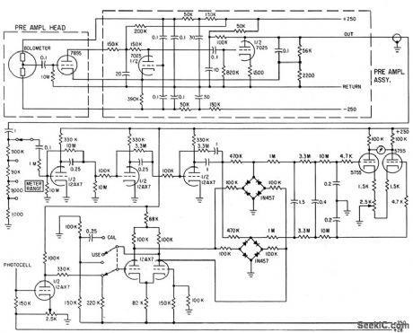
INFRARED_ANALYZER
Published:2009/7/16 3:10:00 Author:Jessie
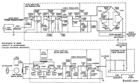
Circuit shows phase-sensitive demodulator, 13-cps amplifier, and modulator of servo system used in Perkin-Elmer Tri-Non triple-beam analyzer for measuring amount of infrared energy absorbed by component of interest in flowing sample of industrial process stream. Servo motor tums variable null-path attenuator to cancel radiation unbalance and restore null-G. C. Carroll, lndustrial Instrument Servicing Hand-book, McGraw-Hill, N.Y., 1960, p 8-51. (View)
View full Circuit Diagram | Comments | Reading(1040)
BOLOMETER_AMPLIFIER_AND_DETECTOR
Published:2009/7/16 3:01:00 Author:Jessie
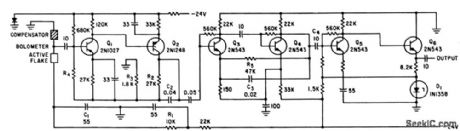
Used in infrared horizon sensor of meteorological satellite. Zener diode D1 provides low-impedance constant-voltage source of bias for detector.-F. Schwarz and W. Chou, Tiros Weather Satellites, Eleatronics, 34:39, p 136-137. (View)
View full Circuit Diagram | Comments | Reading(844)
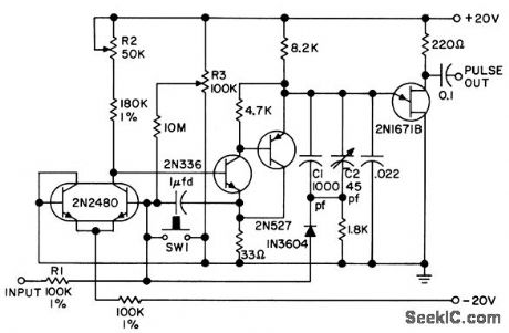
PREFERRED_DISTANCE_MARK_GENERATOR
Published:2009/7/16 2:59:00 Author:Jessie
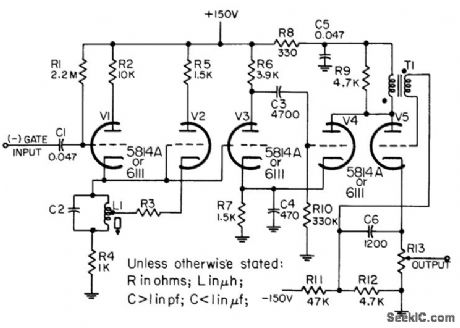
Produces train of accurately spaced pulses. Number of pulses in train is determined by duration of input gate, and distance mark spacing is controlled by values of L1, C2, and R3. R13 is 250 ohms maximum. Output is 0 to 50 v positive, for distance mark spacings of 0.5 to 25 miles in search radar V2 is switched Hartley oscillator, whose output is shaped by mvbr shaper V3-V4, for triggering blocking oscillator VS to produce narrow marker pulses.-NBS, Handbook Preferred Circuits Navy Aeronautical Electronic Equipment, Vol I, Electron Tube Circuits, 1963, PC 55, p 55-2. (View)
View full Circuit Diagram | Comments | Reading(574)
88_108_MC_F_M_CONVERTER_WITH_AFC
Published:2009/7/13 6:45:00 Author:May
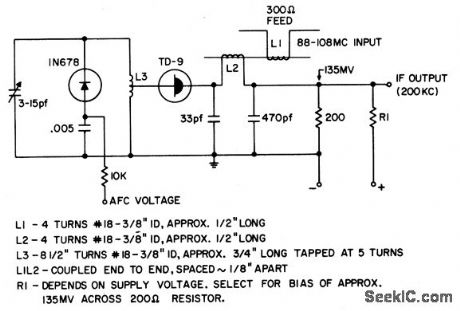
Variable-capacitance diode provides frequency control of tunnel-diode oscillator.- Transistor Manual. Seventh Edition,General Electric Co.1964,P361. (View)
View full Circuit Diagram | Comments | Reading(839)
D_C_TO_AUDIO_FREQUENCY_CONVERTER
Published:2009/7/13 6:39:00 Author:May
Response is nonlinear;1.7V input voltage gives 100 cps;1.9V gives 200 cps; 2.25V gives 400 cps;10V gives 2,000 cps.Output waveform approximates rectangular shape.-D.Busby,Jr.DC to frequency Converter,EEE,10:11,P31. (View)
View full Circuit Diagram | Comments | Reading(692)
VOLTAGE_TO_FREQUENCY_CONVERTER
Published:2009/7/13 6:31:00 Author:May
Out-put frequency is proportional to input voltage, with 1 volt produding 1 kc. Linearity is better than 0.1%.- Transislor Manual, Seventh Edition, General Electric Co.1964, p346. (View)
View full Circuit Diagram | Comments | Reading(0)
VOLTAGE_TO_PULSE_WIDTH_CONVERTER
Published:2009/7/13 6:24:00 Author:May
Converts d-c level linearly to pulse width at preset frequency. Used as switching-type series d-c regulator. C1 is selected to give desired preset frequency, and R10, R11, and R12 are chosen for desired voltage division of input.-M. C. Ellis, Linear Voltage to Duty-Cycle Converter, EEE, 12:3, p72. (View)
View full Circuit Diagram | Comments | Reading(961)
LOW_NOISE_400_MC_CONVERTER
Published:2009/7/13 6:19:00 Author:May
Voltage gain is 36 db, bandwidth 4 Mc, and noise figure only 2.5 db. Uses grounded-grid r-f and mixer stages. Applications include meteor, aurora, and forward scatter propagation studies.-L. F. Garrett, Low Noise Converter for IGY Propagation Study,ELectronics,31;5,p52-54. (View)
View full Circuit Diagram | Comments | Reading(546)
COMPLEMENTARY_RAMPS
Published:2009/7/13 6:15:00 Author:May
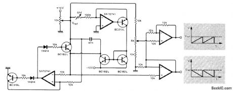
Opamp circuit provides independent controls over amplitude and frequency, as required for amplitude-modulating auditory signals to either ear for creating impression of left to right scan. High output impedance of ramps makes use of voltage follower output stage essential. Another opamp is used for inversion and level-shifting of complementary ramp, so both ramps are available from very low impedance sources. Article describes circuit operation in detail. For values shown, ramp output is variable from 400 mV to 8V, and ramp time from 50 ms to 2 s.-L. J. Retallack, Complementary Ramp Generator with Independent Amplitude/Slope Control, Wireless World, Feb. 1975, p 94. (View)
View full Circuit Diagram | Comments | Reading(847)
| Pages:173/471 At 20161162163164165166167168169170171172173174175176177178179180Under 20 |
Circuit Categories
power supply circuit
Amplifier Circuit
Basic Circuit
LED and Light Circuit
Sensor Circuit
Signal Processing
Electrical Equipment Circuit
Control Circuit
Remote Control Circuit
A/D-D/A Converter Circuit
Audio Circuit
Measuring and Test Circuit
Communication Circuit
Computer-Related Circuit
555 Circuit
Automotive Circuit
Repairing Circuit