
Control Circuit
Index 226
Motor protector 17
Published:2011/6/27 22:18:00 Author:Nicole | Keyword: Motor, protector
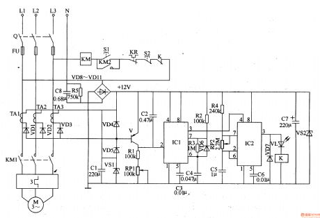
This motor protector circuit is composed of phase pulse detection circuit, monostable trigger circuit, control circuit and power supply circuit, it is shown in the figure 8-53.
The phase pulse detection circuit is made of current transformers TAl-TA3, diodes VDl-VD5, steady voltage diode VS1 and capacitor C1.
The monostable trigger circuit consists of transistor V, resistors R1-R3, potentiometer RP1, capacitors C2-C4, diode VD6 and time base integrated circuit IC1.
The delay control circuit is composed of time base integrated circuit IC2, resistor R4, capacitors C5, C6, diode VD7, LED VL, relay K and AC contactor.
(View)
View full Circuit Diagram | Comments | Reading(737)
Motor protector 18
Published:2011/6/27 22:26:00 Author:Nicole | Keyword: Motor, protector
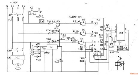
This motor protector circuit is composed of power supply circuit, phase sequence detection circuit, monostable circuit and control implement circuit, it is shown in the figure 8-54.
The power supply circuit is made of power transformer T, rectifier diodes VD1, VD2, capacitors C1, C2 and there terminals steady voltage integrated circuit IC1.
The phase sequence detection circuit consists of diodes VD3-VD5, resistors R1-R10, capacitor C6, four NAND gates Schmitt trigger integrated circuit IC2(D1-D4) and double JK master-slave trigger integrated circuit IC3.
The monostable circuit is composed of resistors R11-Rl3, capacitors C3-C5 and time base integrated circuit IC4.
(View)
View full Circuit Diagram | Comments | Reading(959)
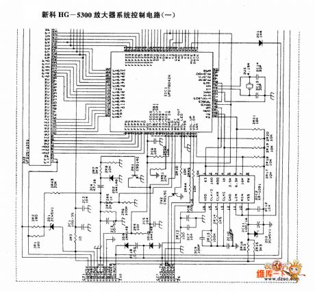
Shinco HG-5300 amplifier system control circuit (a)
Published:2011/7/4 10:59:00 Author:John | Keyword: amplifier system
View full Circuit Diagram | Comments | Reading(1198)
The Sony KV-25G protection circuit
Published:2011/6/15 1:44:00 Author:Christina | Keyword: Sony, protection circuit
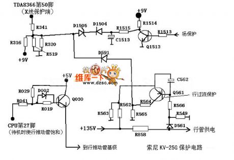
The Sony KV-25G protection circuit is as shown:
(View)
View full Circuit Diagram | Comments | Reading(634)
Motor Control Circuit of VFC320
Published:2011/6/26 5:04:00 Author:Michel | Keyword: Motor Control, Circuit
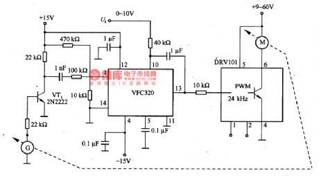
The aboved picture is the motor control circuit composed of VFC320.Tachogenerator G outputs AC current which is correspondent to motor speed.VTl circuit converts it into the narrow negative pulse and trigger frequency/voltage converter VFC320.There are operational amplifiers in VFC320 chip and they are used as the integratorof the speed control loop. When integrator receives the input control voltage of the corresponding average current of equal and opposite direction and the single trigger pulse current added to frequency/voltage converter feedback loop reaches balanced condition.DRVlO1 driver is used in motor and its maximum output current is 1.9 A and which is enough to drive the ordinary motor. (View)
View full Circuit Diagram | Comments | Reading(1441)
The electric switch circuit of touch type (4)
Published:2011/7/4 4:28:00 Author:Seven | Keyword: electric switch circuit, touch type
The following is to introduce an electric switch circuit of touch type which is made of 555 time-based integrated circuit, it characterizes convenient operation(by touching), delaying the auto shut-off and so on, which can be used to control the kitchen ventilator, toilet ventilator and lamps in the stairway, corridor and other place. This electric switch circuit of touch type consists of the touch electrode pole chip A, the time-based integrated circuit IE, the capacitors E1 and C2, the resistance R1 and R2, relay K and so on.
By adjusting the volume of C1, the sensitivity of the single stable trigger can be changed. (View)
View full Circuit Diagram | Comments | Reading(1355)
Practical technique circuit of artificial circuit layout and design
Published:2011/6/30 13:25:00 Author:Sophia | Keyword: Practical technique, Artificial circuit layout and design

(View)
View full Circuit Diagram | Comments | Reading(684)
Water level control circuit
Published:2011/7/2 21:28:00 Author:Lucas | Keyword: Water level , control
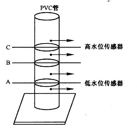
Figure 2-23 (a) shows the sensor. There are two pairs of wires being installed in the corresponding water level A and C inside of the PVC pipe, only when the water level rises more than A, B and C, the pump will stop running. When the water level drops below the C and B, pump will maintain working. Only when the water level is lower than A, the pump is switched on to run. Figure 2-23 (b) shows the pump motor control circuit. In the circuit, Al-A4 use 5V single supplied TLC2274 op amp. Among them, Al and A2 form the comparator to control D flip-flop 7474 and add the reference voltage with about 4V at inverting input end of A3 and A4.
(View)
View full Circuit Diagram | Comments | Reading(1913)
The control circuit of two-phase servo motor
Published:2011/7/2 21:41:00 Author:Lucas | Keyword: control circuit , two-phase , servo motor
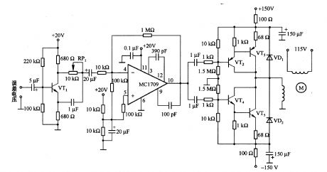
Two-phase servo motor has the field winding and control winding, when the phase difference is 90 °, it generates the rotation torque. The potentiometer connected to the motor shaft will get the voltage difference between the corresponding voltage and target value detected by potentiometer, and voltage difference is used as the error voltage, which is used as the input voltage of servo amplifier to control motor be consistent with the target value. And VTl and its associated components form the phase shift circuit, and MCl709 is the single-end output preamplifier of single power supply, and VT2-VT5 form the B complementary output circuit.
(View)
View full Circuit Diagram | Comments | Reading(5541)
NJM2048 switching regulator control circuit (positive output)
Published:2011/6/30 20:47:00 Author:Lucas | Keyword: switching , regulator , control circuit , positive output
NJM2048 switching regulator control circuit (positive output), main features and pin of DC-DC circuit and power monitor
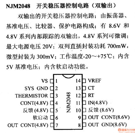
NJM2048 switching regulator control circuit (dual output)
It is the dual-output switching regulator control circuit; it is composed of the oscillator, voltage reference, comparator, protection circuit; it has 8.6V and 4.8V series of internal tracking , 4.8V series can be fine-tuning; maximum supply voltage is 20V; dual-row DIP package power is 700mW, micro-encapsulation is 300mV; Operating temperature is -20 ~ +75 ℃; it includes 5V reference voltage and soft-start function.
(View)
View full Circuit Diagram | Comments | Reading(860)
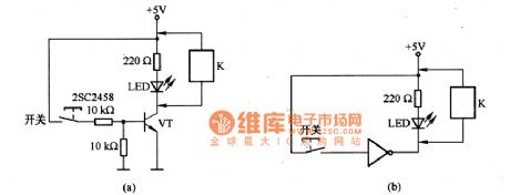
LED(relay) drive circuit diagram
Published:2011/6/30 13:45:00 Author:Sophia | Keyword: LED(relay), drive circuit
(View)
View full Circuit Diagram | Comments | Reading(861)
Mine electric coal drill security power controller circuit diagram
Published:2011/6/13 5:36:00 Author:Lucas | Keyword: Mine , electric coal drill , security power controller
The mine electric coal drill security power controller circuit is composed of the trigger control circuit, maintain control circuit and control implementation circuit, and the circuit is shown as the chart. Trigger control circuit is composed of the drill handle switch S, resistors R1 ~ R5, diodes VD1, VD2, capacitors C1, C2 and transistor V1. Maintain control circuit is composed of the current transformer TA, capacitors C3 ~ C5, diodes VD3, VD4, resistors R6, R7 and transistor V2. Control implementation circuit is composed of the resistors R8, R9, capacitor C6, transistor V3, diode VD5, AC contactor KM and relay K. R1 uses 1 ~ 2W metal film resistor; R2 ~ R9 select 1/4W metal film resistors.
(View)
View full Circuit Diagram | Comments | Reading(540)
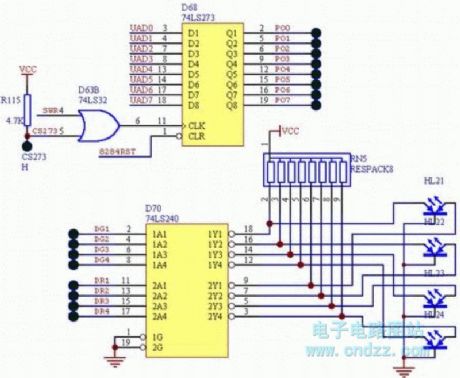
Traffic light control circuit
Published:2011/6/29 20:07:00 Author:zj | Keyword: Traffic light, 74LS273, 74LS240
View full Circuit Diagram | Comments | Reading(2387)
Voltage-Regulator Diode Performance Quick Test Circuit Diagram
Published:2011/6/26 6:12:00 Author:Vicky | Keyword: Voltage-Regulator Diode Performance Quick Test
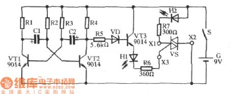
As shown in the picture, VT1 & VT2 etc constitute astable free-running multivibrator and the vibrator’s frequency is determined by C1, R2,R3, C2 etc. The cycle of the vibrator is about 4 seconds. VT2 gives out high level, the level then is transformed by VD, and VT3 is conducted, meanwhile the current is limited by luminous diode H1 and resistance R6, and finally it triggers bidirectional diode thyristor. A good thyristor is immediately conducted, and luminous diode H2 gives out light; when VT2 gives lout low level, VD, VT3, VS all end and H2 is lightless. If H1 and H2 shines synchronously , the thyristor is good; if H1 shines while H2 is extinct, then VS suffers internal short-circuit; if H2 remains luminous all the time, then VS suffers internal breakdown; if both H1 and H2 don’t shine, then VT1 and VT2 circuit don’t vibrate. (View)
View full Circuit Diagram | Comments | Reading(931)
Photosensitive alarm circuit
Published:2011/7/4 4:01:00 Author:Christina | Keyword: Photosensitive alarm
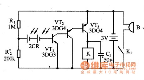
The photosensitive alarm circuit is as shown in the figure. The R1 and R2 are the partial voltage bias circuits. When there is no illumination, the silicon photocell will not produce the voltage, it only the resistance which is connected in the base circuit of the amplifier. When there is the illumination, the silicon photocell will produce the voltage, this voltage and the ground voltage add to the base electrode of VT1 together, so the VT1, VT2 and VT3 conduct, the relay K starts working, the contact point closes, the buzzer sends out the alarm.
This alarm circuit can be used in the anti-theft alarm of the drawer cabinet.
Figure:Photosensitive alarm circuit (View)
View full Circuit Diagram | Comments | Reading(616)
Two-way thyristor AC voltage regulation circuit
Published:2011/7/4 1:31:00 Author:Christina | Keyword: Two-way thyristor, AC, voltage regulation
The two-way thyristor AC voltage regulation circuit is as shown in the figure. Because the thyristor is working in the AC circuit, both of the positive and negative phases can be conductd, so the main circuit is more simple than the unidirectional thyristor regulation circuit. Also you can change the conduction angle to achieve the purpose of regulating.
The light regulation desk lamp circuit which uses the two-way thyristor is as shown in the figure. When the switch S closes, the AC city electricity charges the capacitance C2 through the incandescent bulb, L, RP and R. When the voltage of C2 increases to the conduction voltage of the bi-polar tube, the VD conducts to trigger the two-way thyristor to conduct.
(View)
View full Circuit Diagram | Comments | Reading(1725)
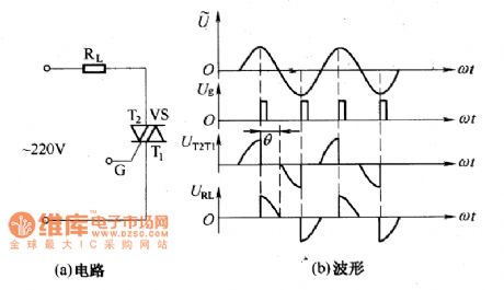
Unidirectional thyristor AC voltage regulation circuit
Published:2011/7/4 1:18:00 Author:Christina | Keyword: Unidirectional thyristor, AC, voltage regulation
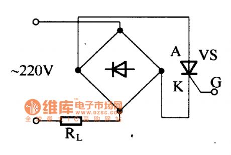
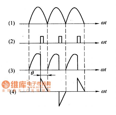
The unidirectional thyristor AC voltage regulation circuit is as shown in the figure a. The load RL is connected in the AC return circuit, the current which flows through it is controlled by the unidirectional thyristor VS's conduction and cut-off. The AC voltage is rectified and is changed into the unidirectional pulsating voltage UAK, as the figure (1) shows. You can change the AC voltage effective value of load Rl by changing the unidirectional thyristor conduction angle θ to achieve the purpose of alternating voltage regulation.
Figure (b) shows one kind of household appliances pressure regulating device, it can be used in the thermoregulation of the electric blanket and the electric iron, also it can be used in the dimming of the table light.
(View)
View full Circuit Diagram | Comments | Reading(1226)
Unijunction transistor delay circuit
Published:2011/7/4 19:30:00 Author:Christina | Keyword: Unijunction transistor, delay circuit
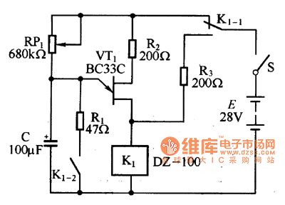
The delay circuit which is composed of the unijunction transistor is as shown in figure 1. When the power supply is connected, the +28V power adds to the unijunction transistor delay circuit through the normally closed contact point of the conversion contact point K1-1 of the relay K1, so the delay circuit starts working. The capacitance C is charged through RP1, when the charging voltage Vc of the C is the same as the peak voltage of the unijunction transistor, the VT conducts, the C discharges through VT and K1, so the discharging current is large, the relay K closes, the normally open contact point of the conversion contact point K1-1 closes, and the normally closed contact point cuts off, the power of the timing circuit turns off.
Figure 1 The delay circuit
(View)
View full Circuit Diagram | Comments | Reading(1312)
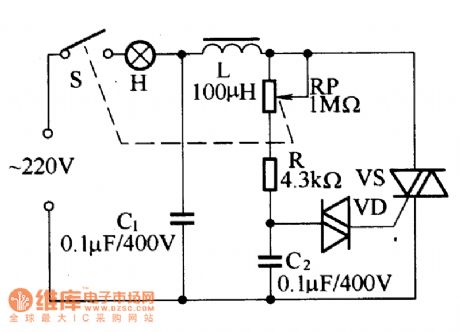
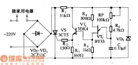
Light control flashing warning light circuit
Published:2011/7/4 7:32:00 Author:Christina | Keyword: Light control, flashing, warning light
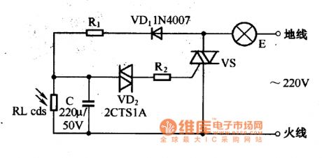
The light control flashing warning light will automaticly turn off, and at night ,the light will automaticly turn on.
The light control flashing warning light circuit is as shown in the figure. When the power is connected, the 220V city electricity will be half wave rectified by the diode VD1, and it charges the C through R1, so the charging current is small, the warning light E will not turn on. The voltage of capacitance C depends on the R1 and the partial voltage value of the photoconductive resistance RL.
In the day time, the photoconductive resistance RL is illuminated by the natural light source, so it has the low resistance, the charging voltage of the capacitance C will not exceed the turning voltage of the two-way trigger diode VD.
Light control flashing warning light circuit (View)
View full Circuit Diagram | Comments | Reading(770)
Sound control photosensitive delay switch circuit
Published:2011/7/4 6:40:00 Author:Christina | Keyword: Sound control, photosensitive, delay, switch circuit
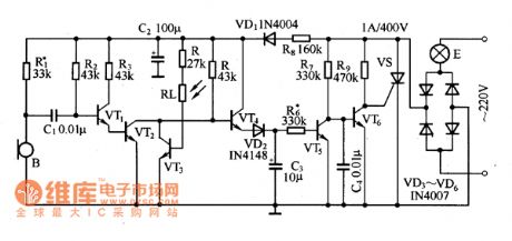
Figure:Sound control photosensitive delay switch circuit
The sound control photosensitive delay switch circuit is as shown in the figure. In the daytime, the photoconductive resistance RL is irradiated by the light, so it is in the low impedance state to conduct the semiconductor tube VT3, so the VT4 and VT5 cut off, the VT6 conducts, the thyristor VS cuts off, the bulb E is in the off state. Because the VT3 is in the conduction state, so no matter what the sound is, the bulb E will not turn on.
At night ,there is no light, so the photoconductive resistance's internal resistance increases to make the VT3 in the cut-off state. If there is no sound, the circuit is the same as the circuit of the daytime; when there is the sound, the microphone B receives the sound signal and changes it into the electrical signal. (View)
View full Circuit Diagram | Comments | Reading(1041)
| Pages:226/312 At 20221222223224225226227228229230231232233234235236237238239240Under 20 |
Circuit Categories
power supply circuit
Amplifier Circuit
Basic Circuit
LED and Light Circuit
Sensor Circuit
Signal Processing
Electrical Equipment Circuit
Control Circuit
Remote Control Circuit
A/D-D/A Converter Circuit
Audio Circuit
Measuring and Test Circuit
Communication Circuit
Computer-Related Circuit
555 Circuit
Automotive Circuit
Repairing Circuit