
Control Circuit
Index 235
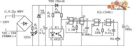
The money-locker or closed chamber anti-pry alarm circuit
Published:2011/6/29 6:32:00 Author:Seven | Keyword: money-locker, closed chamber, anti-pry
See as the figured circuit, it consists of the chamber linked switch SB, electric switch, light control sound circuit and audio amplifier, etc. If it is fixed in a closed chamber or money-locker, when the chamber or locker is pried, the circuit will make purring alarm sound, so the thief will retreat.
(View)
View full Circuit Diagram | Comments | Reading(836)
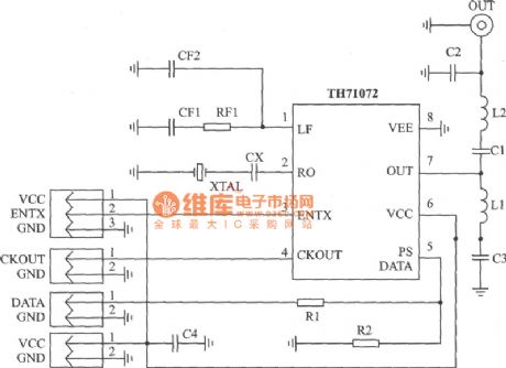
FSK 433MHz Emitter Circuit Diagram
Published:2011/6/19 7:23:00 Author:Vicky | Keyword: FSK 433MHz Emitter
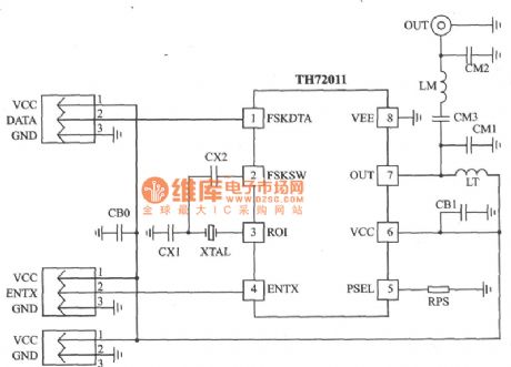
TH72011 applied circuit
TH71072 is a monolithic emitter chip which reaches standards of EN 300 220 and the analogs. It is available for keyless entering system, remote control/remote measuring system, data communication sysytem and security sysetem etc.
Main technical features are as follows:
·Completely integrated and stable PLL;
·Work frequency:380~450 MHz;
·Single-ended RF output;
·FSK modulation mode;
·FSK carrying out modulation driven by crystal oscillator, FSK modulation rate: DC~40 Kb/s;
·Voltage of power supply: 1.9~5.5 V;
·Work current: 3.5~10.7 mA,stand-by current 0.1μA;
·Output power: -l2~+8.5 dBm. (View)
View full Circuit Diagram | Comments | Reading(1134)
The 4-line burglar-proof alarm circuit
Published:2011/6/29 20:47:00 Author:Seven | Keyword: burglar-proof alarm
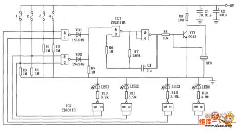
The 4-line burglar-proof alarm circuit is shown in the figure, which consists of the CD40118 integrated chips, it belongs to the multi-line burglar-proof alarm, and it can be used in 4-line burglar-proof alarm spots. It can not only make alarm sounds, but also indicate the monitored 4-line burglary in the term of LED. (View)
View full Circuit Diagram | Comments | Reading(1093)
ASK 440~310MHz Emitter Circuit Diagram
Published:2011/6/19 7:26:00 Author:Vicky | Keyword: ASK 440~310MHz Emitter
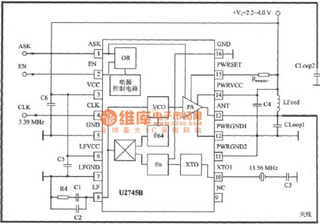
U2745B is a PPL emitter chips specially designed for low-cost data communication, which is available for application in wireless temperature measuring, keyless keyboard, gate lock, light, fan, air-conditioner, shutter control and other consumer products.
Main technical features are as follows:
·Emitter frequency: 310~440 MHz;
·ASK modulation mode;
·Voltge of power supply: 2.2~4 V;
·Maximum output power: 5 dBm(Vs=3 V,f=433.92 MHz,RPWRSET=l.2 kΩ);
·Maximum power dissipation: 250 mW;
·Maximum work current: l2.5 mA,maximum current udner low-power dissipation mode 10μA;
·Maximum data transfer rate: 20 Kb/s;
·Microprocessor clock signal ,which can be compatible with microcontroller such as M44C090 and M44C890;
·ESD protection (excluding pins XT02 and XT01)as requested by MIL-STD.883(4KV HBM);
·Work temperature: -20~+70℃. (View)
View full Circuit Diagram | Comments | Reading(1401)
The power-off alarm circuit of passive type
Published:2011/6/29 6:45:00 Author:Seven | Keyword: power-off, alarm circuit, passive type
The power-off alarm of passive type doesn't mean it doesn't need a working power supply, but is makes use of the electricity in the capacitor, which allows the alarm to work for some time and complete the power-off informing task, the circuit is shown in the figure.
(View)
View full Circuit Diagram | Comments | Reading(787)
ASK/FM 433/315 MHz Emitter Circuit Diagram
Published:2011/6/19 7:29:00 Author:Vicky | Keyword: ASK/FM 433/315 MHz Emitter
TH71071 applied circuit
TH71071 is a monolithic emitter chip which reaches standards of EN 300 220 and the analogs. It is available for keyless entering system, remote control/remote measuring system, data communication sysytem and security sysetem etc.
Main technical features are as follows:
·Work frequency range: 310~440 MHz;
·ASK/FM modulation mode;
·ASK is conducted by interior power amplifier/gained by closing keying
·FM which makes use of externally-linked variode
·Voltage of power supply: 2.2~5.5 V;
·Work current: 4.8~11.5 mA, maximum stand-by current: 0.1μA;
·Output power: -12~+2 dBm. (View)
View full Circuit Diagram | Comments | Reading(912)
FM Emitter Module Circuit Diagram
Published:2011/6/19 7:59:00 Author:Vicky | Keyword: FM Emitter Module
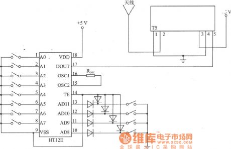
T5 is a micro UHF emitter module and is used with receptor module R5. It is suitable for application in one point to one point or multipoint connection, such as vehicle warning system, remote control of warehouse gate and house & commerce security system.
Main technical features are as follows:
·Work frequency: 433.92 MHz;
·Data transfer rate up to l28 Kb/s;
·Emitting distance up to 300 m;
·Voltage of power supply: 4.5~5.5 V;
·Maximum work current: l2 mA;
·Maximum RF power: +12 dBm. (View)
View full Circuit Diagram | Comments | Reading(737)
Capacitive closing switch circuit composed of the division devices
Published:2011/6/24 23:46:00 Author:TaoXi | Keyword: Capacitive closing switch, division devices

The capacitive closing switch circuit is composed of a RF oscillator circuit and a detection board. The capacitive sensing type controller principle diagram (composed of the division devices) is as shown in the figure.
In the figure, the RF oscillator circuit is composed of the transistor VT1 and the surrounding components; the metal induction electrode plate is connected with the collector of VT1 that can be used as the detector. When there is no conductor closing the induction electrode plate, the oscilation circuit which is composed of the VT1 oscillates normally, at this time the RF voltage signal which is output by the VT1 emitter is changed into the DC control signal after it is detected by VD1 and VD2, this signal conducts the switching tube VT2, the relay closes to connect the power supply of the controlled circuit.
(View)
View full Circuit Diagram | Comments | Reading(1394)
TTL server control circuit
Published:2011/6/19 19:13:00 Author:TaoXi | Keyword: TTL, server, control circuit
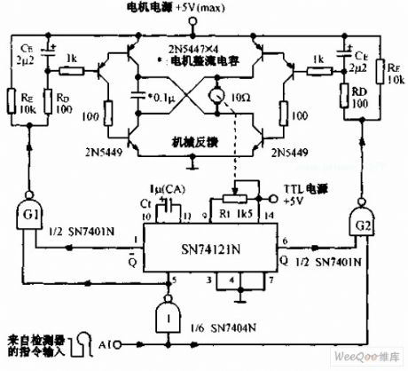
The TTL server control circuit can be used in the 9-channel control system. This system has 9 same servos, the decoder of the data transmission line (DTL) receiving port sends the signal to the servo, the command pulse controls the rotation direction and the rotation duration of the electromotor.
(View)
View full Circuit Diagram | Comments | Reading(799)
Radio Frequency Modulator Circuit Diagram
Published:2011/6/19 9:11:00 Author:Vicky | Keyword: Radio Frequency Modulator
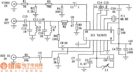
The above picture is the detailed circuit of radio frequency modulator. IC1 is integrated circuit TA7673 especially for modulator, the pins 10 & 11 of which produce picture carrier signal by externally connection to crystal oscillator, and pins 4 & 5 of which produce 6.5MHz secondary audio signal. Audio signal is input via pin 6 of ICl, and video signal is input via pin 16 of ICl. When crystal oscillators of different work frequency are connected to part between pin 10 and pin 11 , the circuit can then give out picture carrier signal from channel 1 to 5 in pin 2 and pin 15. The circuit doesn’t need debugging after finishing assembly, but the whole circuit uses small metal-box as shield. (View)
View full Circuit Diagram | Comments | Reading(1721)
555 simple TV channels transformation remote controller circuit
Published:2011/6/15 20:54:00 Author:TaoXi | Keyword: 555, simple, TV channels, transformation, remote controller
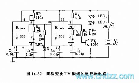
This remote control circuit uses the dual time base circuit 556 as the core, the circuit is as shown in figure 14-32.
In this figure, the astable multivibrator is composed of the IC1-a (1/2 NE556) and R2, RP1, C1, the oscillation frequency f1=1.4/(RP1+2R2)C1, you can make the resonance frequency to 1Hz by adjusting RP1. The output of it supplies the trigger pulse to the IC1-b(1/2NE556) time base circuit. The audio oscillator is composed of the IC1-b and R4, R5, C4. When there is the high level pulse, the audio oscillator starts working, the oscillation frequency f2=1.44/(R4+2R5)C4, the oscillation frequency of the figure parameters is about 2kHz. The pulse sequence is drived by VT1 to make the infrared launch tube LED to send out the 2kHz infrared modulation light.
(View)
View full Circuit Diagram | Comments | Reading(783)
555 simple electronic keyboard circuit
Published:2011/6/15 19:12:00 Author:TaoXi | Keyword: 555, simple, electronic keyboard
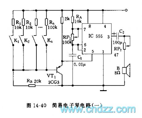
As the figure 14-40 shows, the controllable multivibrator is composed of the 555 and RA, RP1, C1, the oscillation frequency is related with the control voltage (pin-5), but the voltage of pin-5 depends on the partial voltage of R1~Rn and RB, and it is related with the conduction situation of VT1. The VT1 works in the amplifier region, voltage of electrode c is in the range of 3-6V, the control port pin-5 has a corresponding voltage value and it outputs the frequency of one scale or half scale. The lower the control voltage is, the higher the frequency is, but the control voltage is not less than 0.7V. When debugging, you need to adjust it repeatedly to distinguish the scales and notes. Any one of the resistors R1 ~ Rn can get the suitable resistance by using the series or parallel methods.
(View)
View full Circuit Diagram | Comments | Reading(2741)
The 2A step-down DC switching power supply made of efficient switch controller LT1148-5
Published:2011/6/15 7:11:00 Author:Borg | Keyword: step-down, power supply, switch controller
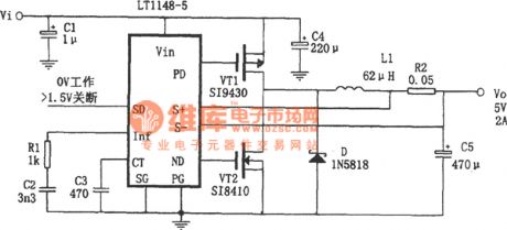
In the figure is a 2A step-down DC switching power supply made of efficient switch controller LT1148-5. The power supply circuit in fixed with MOSFET as the controlled power switch element, which replaces the external Schottky subsequent flow diode, so the voltage drop and the power consumption can be reduced further, and the switching efficiency of the power supply is increased. In the figure, if the input voltage is 6V, the loading current ranges from 20mA to 1.8A, the switching efficiency is over 95%, and the diode D functions as the protector. (View)
View full Circuit Diagram | Comments | Reading(627)
The Doppler security alarm circuit
Published:2011/6/27 20:32:00 Author:Borg | Keyword: Doppler, security alarm
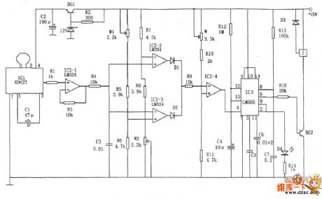
In the figure is the Doppler security alarm circuit. This circuit consists of the voltage comparator, Doppler effect sensor integrated circuit, trigger single steady and time delay circuit and so on. The chip IC3 is made of the dual time-based circuit 556, half of which composes the single steady trigger with R13 AND C7, the other half composes the single steady time delay circuit with R12 and C4, the delayed time is td=1.1R12C4, the delayed time according to the figured parameter is about 10s, which makes the master have enough time to leave the spot. The chip IC2 is adopted with the 4-op-amp LM324. IC2-2 and IC2-3 compose the window comparator.
(View)
View full Circuit Diagram | Comments | Reading(1154)
The wireless alarm circuit with language chip
Published:2011/6/27 20:43:00 Author:Borg | Keyword: wireless alarm circuit, language chip
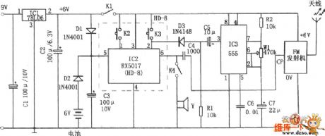
In the figure is the wireless alarm circuit with language chip. The alarm consists of the FM emitter, time-based circuit 555, regulated circuit and the language storage composed of the chip RX5017. In the figure, 555, R2, W1 and C7 compose the astable multi-resonance oscillator, whose frequency is f=l.44/(R1+Rwl)C7 which can be changed by adjusting W1. IC2 is the language chip RX5017, 3-pin is the power supply terminal, 5-pin is the maintain terminal of info storage, all of which are connected with the 6V battery by D2 to avoid power-off, 2-pin is the recording trigger terminal.
(View)
View full Circuit Diagram | Comments | Reading(885)
The automatic for help alarm circuit
Published:2011/6/27 21:07:00 Author:Borg | Keyword: for help, alarm, automatic
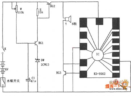
In the figure is the automatic for help alarm circuit. The circuit composes of the music integrated circuit IC(KD-9562), regulated pipe DW(2CW13), mercury switch, transistor, sliding rheostat W and the power supply, etc. It can be packaged in a plastic box and then put in the pocket, or fixed in the cane. When the person is erected, the mercury switch is off, the power supply is cut off, the circuit is not working and the music integrated circuit IC is silent. When the person is banding down (the alarm in the pocket) or the cane is falling on the ground, the mercury switch is closed.
(View)
View full Circuit Diagram | Comments | Reading(665)
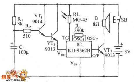
The microwave burglarproof alarm circuit
Published:2011/6/27 21:24:00 Author:Borg | Keyword: microwave, burglarproof alarm
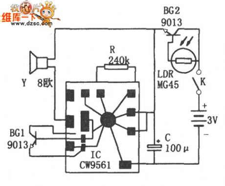
In the figure is the microwave burglarproof alarm circuit. This circuit consists of the simulated sound integrated circuit IC(CW9561), the LDR (MG45), the transistor and the power supply, etc. The alarm is installed in the closable room where there's some light, if the room is closed, the LDR will be in a high resistance because of no light, which makes the transistor BG2 blocked, so the simulated sound integrated circuit CW9561 is power-off, IC is not working, accordingly, the loudspeaker is silent. If the room is open, the LDR is in a low resistance due to the light.
(View)
View full Circuit Diagram | Comments | Reading(607)
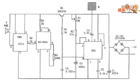
The circuit of the microwave burglarproof alarm
Published:2011/6/27 21:35:00 Author:Borg | Keyword: microwave, burglarproof alarm
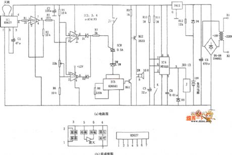
In the figure is the circuit of the microwave burglarproof alarm. This circuit consists of the Doppler FS sensor circuit IC1, the voltage comparator, the trigger single steady and delay circuit, stereo integrated circuit IC5 and so on. When the moving target is coming up, due to the FS between the reflected magnetic wave and the emitting wave, the Doppler FS sensor IC1 will output the DC LEV which is in positive proportion to the Doppler frequency generated when the object is moving, therefore, the detection and alert are done. And the microwave protection area is about 100m. The Doppler FS sensor IC1 is adopted with RD727 module.
(View)
View full Circuit Diagram | Comments | Reading(662)
The ultrasonic wave burglarproof circuit
Published:2011/6/27 21:47:00 Author:Borg | Keyword: ultrasonic wave, burglarproof
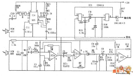
In the figure is the ultrasonic wave burglarproof circuit. The alarm contains the ultrasonic wave emitter and receiver and the decoder. In the circuit, the core of the ultrasonic wave emitter is the multi-resonance oscillator which consists of the 555, R19, R20, R21, W2, C12 and so on, and its oscillating frequency is f=1.44/(R21+Rw2十2R20+R19)C12, the frequency corresponding to the figured parameter is 40kHz+500Hz. After being reversed twice, the alternating square wave output by the oscillator is pushing the ultrasonic sensor UCM40T to output the ultrasonic pulse wave of 40KHz. When the wave encounters the moving object, the Doppler FS is generated.
(View)
View full Circuit Diagram | Comments | Reading(710)
The touch burglarproof alarm circuit
Published:2011/6/27 20:19:00 Author:Borg | Keyword: burglarproof alarm
In the figure is the touch burglarproof alarm circuit. This circuit consists of the single steady trigger, the sound simulating circuit, the audio power supply amplifier circuit, the touching metal chip M, the rectifier filter circuit and so on. In the circuit, the time-based circuit 555, R1, R2 and C4 compose the single steady trigger, whose input signal, i.e the triggering signal past C3 when the touching metal chip M is touched, it is input from 2-pin, and the responding circuit turns into the temporary steady state, then the 3-pin is outputting a high LEV. The high LEV conducts the BG pipe, then it makes the power supply of the next circuit conducting.
(View)
View full Circuit Diagram | Comments | Reading(809)
| Pages:235/312 At 20221222223224225226227228229230231232233234235236237238239240Under 20 |
Circuit Categories
power supply circuit
Amplifier Circuit
Basic Circuit
LED and Light Circuit
Sensor Circuit
Signal Processing
Electrical Equipment Circuit
Control Circuit
Remote Control Circuit
A/D-D/A Converter Circuit
Audio Circuit
Measuring and Test Circuit
Communication Circuit
Computer-Related Circuit
555 Circuit
Automotive Circuit
Repairing Circuit