
Control Circuit
Index 221
The alarm control key circuit
Published:2011/7/6 1:03:00 Author:Borg | Keyword: alarm, control key

This switch will suit the Modular Burglar Alarm circuit. However, it also has other applications. The Keypad must be the kind with a common terminal and a separate connection for each key. On a 12-key pad, look for 13 terminals. The matrix type with 7 terminals will NOT do. Choose the five keys you want as your code, and connect them to 'A, B, C, D & E'. Wire the common to R1 and all the remaining keys to 'F'. Because your choice can include the non-numeric symbols, almost 100 000 different codes are available. The Alarm is set using the first four of your five chosen keys. When 'A, B, C & D' are pressed in the right order and within the time set by C1 and R2 (about 10 seconds), current through R11 switches Q6 on. The relay energizes, and then holds itself on by providing base current for Q6 through R12. The 12-volt output switches from the off to the set terminal, and the LED lights. To switch the Alarm off again it is necessary to press A, B, C, D & E in the right order. The IC is a quad 2-input AND gate, a Cmos 4081. These gates only produce a high output when both inputs are high. Pressing 'A' takes pin 1 high for a period of time set by C1 and R2. This 'enables' gate 1, so that when 'B' is pressed, the output at pin 3 will go high. This output does two jobs. It locks itself high using R3 and it enables gate 2 by taking pin 5 high. The remaining gates operate in the same way, each locking itself on through a resistor and enabling its successor. If the correct code is entered within the time allowed, pin 10 will switch Q5 on and so connect the base of Q6 to ground. This causes Q6 to switch off and the relay to drop out. Any keys not wired to 'A, B, C, D or E ' are connected to the base of Q4 by R9. Whenever one of these 'wrong' keys is pressed, Q4 takes pin 1 low. This removes the 'enable' from gate 1, and the code entry process fails. If C, D or E is pressed out of sequence, Q1, Q2 or Q3 will also take pin 1 low, with the same result. You can change the code by altering the keypad connections. If you make a mistake entering the code, just start again. If you need a more secure code you can use a bigger keypad with more 'wrong' keys wired to 'F'. A 16-key pad gives over half a million different codes. All components are shown lying flat on the board; but some are actually mounted upright. The links are bare copper wires on the component side. Two of the links must be fitted before the IC. (View)
View full Circuit Diagram | Comments | Reading(735)
The doorphone communication circuit
Published:2011/7/6 0:59:00 Author:Borg | Keyword: doorphone, communication circuit
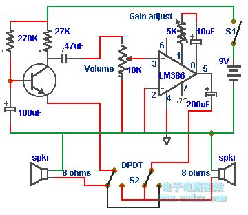
In this doorphone circuit,an 8 ohm speaker is used both as a microphone and also an output device. The BC109C stage amplifies in common base mode, giving good voltage gain , whilst providing a low impedance input to match the speaker. Self DC bias is used allowing for variations in transistor current gain. An LM386 is used in non-inverting mode as a power amplifier to boost voltage gain and drive the 8 ohm speaker. The 10k potentiometer acts as the volume control, and overall gain may be adjusted using the 5k preset. The double pole double throw switch, reverses the loudspeaker positions, so that one is used to talk and the other to listen. Manually operating the switch (from inside the house) allows two way communication. (View)
View full Circuit Diagram | Comments | Reading(879)
The ultra-sonic moving alarm
Published:2011/7/5 22:21:00 Author:qqtang | Keyword: ultra-sonic
View full Circuit Diagram | Comments | Reading(877)
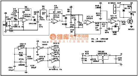
The electric ballast control ML4831 circuit of high power factor and high efficiency
Published:2011/7/5 22:10:00 Author:qqtang | Keyword: ballast control, high power factor
Figure:The electric ballast control ML4831 of high power factor and high efficiency (View)
View full Circuit Diagram | Comments | Reading(626)
ground isolation circuit by optical couplers
Published:2011/7/4 23:44:00 Author:chopper | Keyword: ground isolation, optical couplers
As for some circuits,one point connection between AGND and DGND is very different.Additionally,because of the difference of electric potential of the AGND and DGND in the circuit,the landlines can't be connected.And we adopts optical coupler to separate the AGND and DGND,just as picture.If the signal is transfered in the form of light,then the connection between AGND and DGND is not necessary.
(View)
View full Circuit Diagram | Comments | Reading(603)
The serial connection current expanding circuit of 3-terminal regulated chip
Published:2011/6/24 7:41:00 Author:Seven | Keyword: serial connection, 3-terminal regulated chip
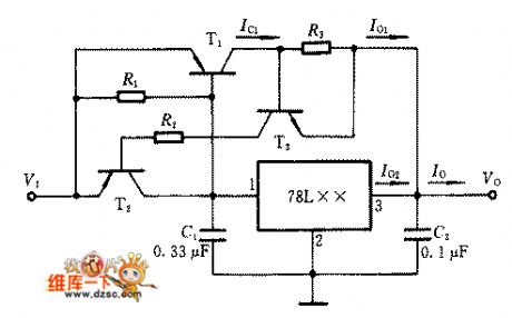
When a current that is higher than 0.1A is needed, we can use other types of integrated circuit the following current expanding circuit. The output current of the 78 series circuit is I0=I01+I02, of which I01=Ic1, I02≈0.7V/R1. This serial connection current expanding circuit of 3-terminal regulated chip has the function of over-current protection, when it is normally working, T2 and T3 are blocked; when IO is over-current, IO1 is increasing, the voltage drop of the current limiting resistor R3 makes T3 and T2 conducting, the VBE of T1 is falling ,which limits the IC1 of T1 and it also protects T1 from being broken of over current.
(View)
View full Circuit Diagram | Comments | Reading(739)
The FM modulation wireless microphone circuit
Published:2011/6/24 7:41:00 Author:Seven | Keyword: FM modulation, wireless microphone
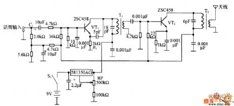
In the figure is the FM modulation wireless microphone circuit, in fact, this is the FM modulation commutator whose frequency is 80~90MHz. The working principle is as follows: the microphone converts the sound signal into the voltage signal which is added on the VT1 basic pole by the coupling capacitor C1, the current in the emitting pole is switched into the voltage, and the voltage change on R1 makes the collecting electrode voltage change, then the capacitor of the collecting pole changes and the oscillating frequency changes, which modulates FM. The modulating signal is emitted after it's been magnified by VT2.
(View)
View full Circuit Diagram | Comments | Reading(1381)
The controllable silicon(thyristor) element equivalent circuit
Published:2011/6/24 7:40:00 Author:Seven | Keyword: controllable silicon, equivalent circuit
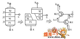
The controllable silicon(thyristor) is a 4-layer, 3-terminal element, which has 3 PN knot, when analysing its principle, we can regard it as an element composed of a PNP and a NPN, its equivalent chart is in figure 1.
When the positive pole A is added with a forward voltage, BG1 and BG2 are both in amplifying state. At the moment, if we input a positive trigger signal from the control pole G, then BG2 will have a basic current ib2 in it, after the current is amplified by BG2, the collecting electrode current is ic2=β2ib2. As the collecting electrodes of BG2 and BG1 are connected directly, so ib1=ic2. (View)
View full Circuit Diagram | Comments | Reading(683)
The gas fog alarm circuit
Published:2011/6/24 8:04:00 Author:qqtang | Keyword: gas, fog alarm
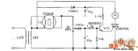
See as the figure, when there is combustible gas. The conductance of TGS308 gas sensor is increasing, the voltage is picked out by the potentiometer RP1 floating spot, and its value rises to 20v from the normal 3V effectively. The risen voltage is added to the transistor VT1 by the diode and the 4.7kΩ resistor, which makes VTI conducting, and the dual-direction transistor 2N6070A is conducting with VT1. Therefore, the full-wave AC conductance H generates a sound of 90dB, which fulfills alarming. H is a 20V AC alarm of De1taJ6003168. When the gas disappears from the sensor, the circuit gets to it primary state.
(View)
View full Circuit Diagram | Comments | Reading(661)
The light control switch circuit of LDR
Published:2011/6/28 7:53:00 Author:qqtang | Keyword: light control switch, LDR
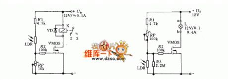
The power switch can be made of power MOS FET and the sensitive element can be the LDR. The light is shed on the LDR, it is in low resistance and there is a signal on the grid of the sound effect transistor, the source-drain is conducting, so the state of the relay is changed by K, which generates sounds and fulfills the control function. If the LDR is fixed at the low LEV sector, there won't be light on the LDR when it's dark outside, so the resistance of the LDR is high and the grid of the VMOS pipe is high, which makes the lamp L light.
(View)
View full Circuit Diagram | Comments | Reading(1261)
The TD-5 ultra-sonic micro fog humidifier circuit
Published:2011/6/24 8:02:00 Author:qqtang | Keyword: ultra-sonic, fog humidifier
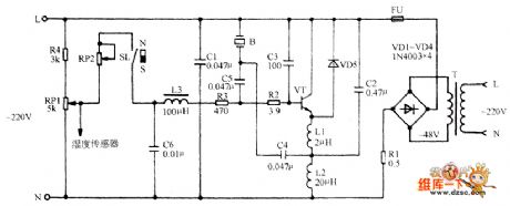
T-power supply transformer FU-fuse VT-triode L1,L2,L3-the inductor B-voltage pottery power switch S-N-magnet ring buoy SL-water level switch
RP1-fog volume control switch RP2-adjustable resistor
(View)
View full Circuit Diagram | Comments | Reading(1408)
Motor speed control circuit composed of NE556
Published:2011/7/2 21:49:00 Author:Lucas | Keyword: Motor speed, control
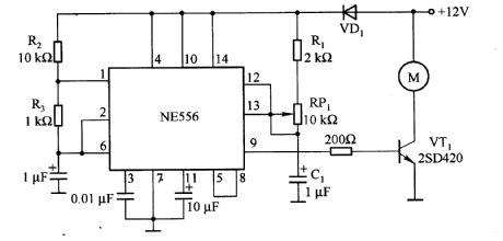
NE556 chip has two timers with exactly the same functions: one timer is the astable multivibrator circuit, of which output is used as the trigger signal; the other is the monostable multivibrator circuit, of which time constant is adjusted by RP1. It constitutes the motor control circuit with constant frequency and adjustable duty cycle. Oscillation frequency f = 1.44 / [(R2 +2 R3) Cl], the duty cycle D = [1.6 (Rl ten R (RP1) Cl] [(R2+ 2R3) C1]. The small duty cycle will start the moyor. VTl uses 2SD42O transistor with Ic = lOA, h (EF) in 1000 or more to directly drive motor.
(View)
View full Circuit Diagram | Comments | Reading(5807)
Positioning control circuit composed of μA709
Published:2011/7/1 21:26:00 Author:Lucas | Keyword: Positioning control
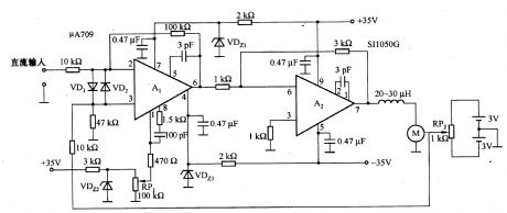
In the circuit, Al gain is about 10 times, and the total circuit gain is about 30 times. Supply voltage is ± 35V. Al's power supply voltage is 13V, which is stabilized by VDz1 and VDz2 voltage-regulator tube from ± 35V. RP1 is used to adjust the offset voltage of A1. When the input voltage is zero, adjusting RPl can make the position is section start. If the input is connected to D / A converter, you can use digitto locate position.
(View)
View full Circuit Diagram | Comments | Reading(776)
Motor control circuit composed of NE555
Published:2011/7/1 21:29:00 Author:Lucas | Keyword: Motor control
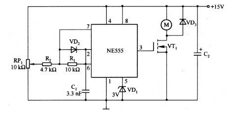
Oscillation frequencyis decidedby the capacitor Cl, resistor Rl and so on, according to the chart component parameters, the oscillation frequency is 20 to 50KHz,and the withstand voltage of VT1 is 5OV. Using BUZll cancontrol the motor current in 2OA.
(View)
View full Circuit Diagram | Comments | Reading(11222)
Motor positive, reversal rotation control circuit composed of MOSFET
Published:2011/7/1 22:42:00 Author:Lucas | Keyword: Motor, positive, reversal, rotation control , MOSFET
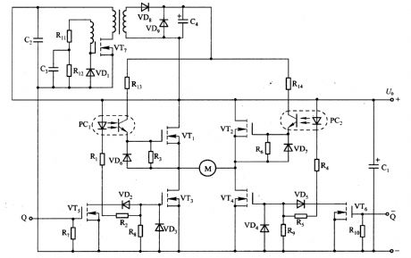
Plus signal ˉ Q can drive the left and right bridge to control the motor positive, reversal rotation. When Q input is in high level, VT5 is conducted, and VT3 is quickly stopped by VD2. Rl can limit the diode current in PCl, so VTl is conducted after delaying several μs. If ˉ Q input is in low level, then VT6 is stopped, and the current flowing VD4 rapid decreases, then the optical coupler PC2 is stopped. R6 resistor make VT2 deadline, then the power charges to the gate of the VT4 and make it turn on by VD4, R4 and R5.
(View)
View full Circuit Diagram | Comments | Reading(1344)
555 home appliance dual-purpose timer circuit
Published:2011/6/13 20:25:00 Author:TaoXi | Keyword: 555, home appliance, dual-purpose, timer
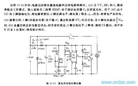
As the figure 15-16 shows, the circuit is composed of the step-down rectifier circuit and the timing circuit. The monostable operating mode is composed of the 555, VT1, RP1 and C3. You can add the field-effect transistor 3DJ6F to ensure the capacitor C3 is charged with the constant-current. If you press AN, the circuit is set because the pin-2 of 555 connects with the ground potential, pin-3 has the high electrical level, the relay J and J1-1 close to supply power to the home appliances.
After the 555 is set, the pin-7 is in the opening circuit state, C3 charges pin-7 through the constant current source VT1, when pin-6's voltage is higher than 2/3VDD, the 555 is from the set state to the reset state.
(View)
View full Circuit Diagram | Comments | Reading(908)
555 reading-newsstand automatic floodlight circuit
Published:2011/6/13 20:25:00 Author:TaoXi | Keyword: NE555, automatic, floodlight
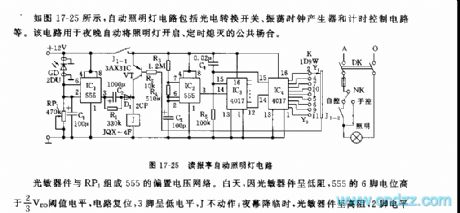
As the figure 17-25 shows, the automatic floodlight circuit is composed of the optoelectronic multiplex switch circuit, the oscillation clock generator and the timer control circuit.etc.
The 555 offset voltage network is composed of the photodetector and the RP1. In the daytime, the photodetector has the low resistance, the electric potential of 555's pin-5 is higher than 2/3VDD threshold level, the circuit resets, pin-3 has the low level voltage, J failure to actuate, At night, the photodetector has the high resistance, pin-2's electrical level is lower than 1/3VDD, 555 sets, pin-3 has high level voltage, J closes and the light turns on.
The timing power-off circuit is composed of the IC2~IC4 and the VT. The ultra-low frequency astable multivibrator is composed of the IC2(555) and R3,R4,R5.
(View)
View full Circuit Diagram | Comments | Reading(653)
555 water temperature alarm circuit
Published:2011/6/13 20:26:00 Author:TaoXi | Keyword: 555, water temperature, alarm circuit
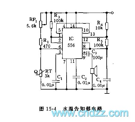
As the figure 15-4 shows, this circuit uses the 556 as the core. The monostable trigger is composed of the left part (1/2 556) of IC, the R1, R3, RP1 and the thermistor probe. The thermistor uses the resistance which has the RT=3kΩ and the negative temperature coefficient. When the water temperature is 100 degrees celsius, the resistance value is about 240Ω; when the water temperature is 50 degrees celsius, the resistance value is about 950Ω. If you pre-set the temperature and adjust RP1 to 50Ω, so the VA=RT/(RP1+R1+RT)<1/3, when the trigger port pin-6's electric potential is lower than 1/3VDD, the trigger is set, the high electrical level which is output by the pin-5 adds to the right part of the 1/2 556's reset port, f=1.44/(R4+2R5)C4, the oscillation frequency is about 1000Hz.
(View)
View full Circuit Diagram | Comments | Reading(1277)
Door alarm circuit with the time recognition function composed of the NE555
Published:2011/6/14 2:45:00 Author:TaoXi | Keyword: Door alarm, time recognition
Door alarm circuit with the time recognition function (View)
View full Circuit Diagram | Comments | Reading(623)
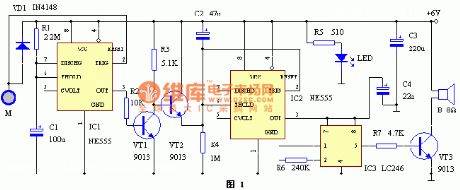
555 automatic water supply circuit with the magnetic card to get water
Published:2011/6/13 20:27:00 Author:TaoXi | Keyword: 555, automatic, water supply circuit, magnetic card
This circuit is composed of the step-down rectifier circuit, the magnetic control trigger and relay control electromagnetic valve circuit.etc, as the figure 15-41 shows.
The HG is the reed pipe magnetic control switch, it is usually in the disconnected state, the monostable delay circuit is composed of the HG, 555, RP1, R2 and C2, the charging voltage (>2/3VDD) of C2 makes the 555 in the reset state, the relay K will not work. If the user put the magnetic card into the entrance, when the magnetic card gets through the reed pipe HG, the contact point closes, the pin-2's low electrical level of the 555 sets the 555, the pin-3 has the high electric potential, the relay K gets power to close, the contact point K1-1 closes too, the electromagnetic valve DF opens to prevent the water.
(View)
View full Circuit Diagram | Comments | Reading(815)
| Pages:221/312 At 20221222223224225226227228229230231232233234235236237238239240Under 20 |
Circuit Categories
power supply circuit
Amplifier Circuit
Basic Circuit
LED and Light Circuit
Sensor Circuit
Signal Processing
Electrical Equipment Circuit
Control Circuit
Remote Control Circuit
A/D-D/A Converter Circuit
Audio Circuit
Measuring and Test Circuit
Communication Circuit
Computer-Related Circuit
555 Circuit
Automotive Circuit
Repairing Circuit