
Circuit Diagram
Index 1226
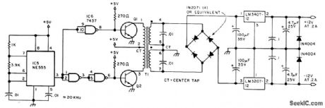
_8_V_FROM__5_V
Published:2009/6/30 2:26:00 Author:May
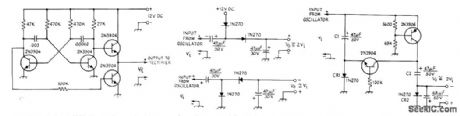
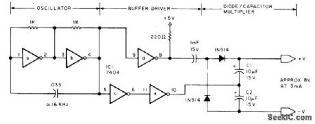
Oscillator operating atabout 16 kHz steps up 5-V supply voltage of microprocessor to 8 V for driving special interface circuits. Sections c,d,and e of 7404 hex inverter form buffer and driver for voltage-dou-bling rectifier.—S. Ciarcia,Build a 5 W DC to DC to DC converter,BYTE,Oct.1978, p22, 24, 26, 28, and 30-31. (View)
View full Circuit Diagram | Comments | Reading(1893)
FLUITER_METER
Published:2009/6/30 2:25:00 Author:May
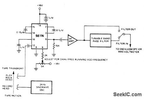
Signetics 561N PLL detects frequency variations in 3-kHz tone recorded on magnetic tape for test purposes. Frequency of VCO in 561N is set to nominal 3kHz with 5K pot.Demodulated output is AC coupled to amplffier having high input impedance. Either CRO or true PMS voltmeter can be used to make RMS flutter readings. To calibrate circuit, feed in 3-kHz tone from oscillator and measure output level shift when frequency is offset 1%.- Sig-netics Analog Data Manual, Signetics, Sunnyvale, CA 1977, p 860. (View)
View full Circuit Diagram | Comments | Reading(776)
DC_MULTIPLIERS
Published:2009/6/30 2:25:00 Author:May
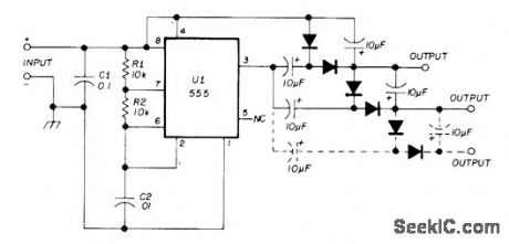
Voltage output from positive voltage booster (+12 VDC to +20 VDC) is increased by using diode-capacitor voltage-doubler sections as shown. Diodes are 1N914, 1N4148, or equivalent. Doubling is achieved at expense of available current. Same technique may be used to increase output of DC/DC converter having negative output voltage.—G. A. Graham, Low-Power DC-DC Converter, Ham Radio, March 1975, p 54-56. (View)
View full Circuit Diagram | Comments | Reading(3976)
_5_V_TO__7_V
Published:2009/6/30 2:24:00 Author:May
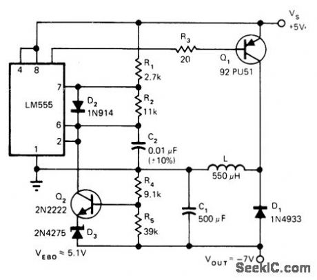
Uses LM555 timer as variable-duty-cycle pulse generator controlling transistor switchQ1 which in turn drivesflyback circuit.Regulator Q2-D3-R4-R5 varies duty cycle according to load, and flyback circuit L-D1-C1 develops negative output voltage. When Q1 is on, current flows through L to ground. When Q1 turns off, polarity across L reverses, diode becomes forward-biased, and negative voltage appears across C1 and load. When Q1 turns on again, voltage across L reverses for start of new cycle. Circuit eliminates separate transformer supply for negative supply of microprocessor. Efficiency is about 60%, load regulation 1.3%, and supply rejection 30 dB. Article gives design equations.—P. Brown, Jr., Converter Generates Negative μP Bias Voltage from +5V, EDN Magazine, Aug.5, 1977, p 42, 44, and 46. (View)
View full Circuit Diagram | Comments | Reading(1594)
_15_V_FROM__15_V
Published:2009/6/30 2:22:00 Author:May
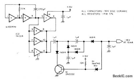
First two sections, of 74C04 hex inverter form 100-kHz oscillitor, with other sections connected to provide inversion of standard microprocessor source voltage as required for some interfaces and some DA converters.Shunt regulator formed by D1 and Q1 maintains output vottage relatively constant.Changing zener D1 to 13 V makes output -12 V.—S. Ciarcia, Build a 5 W DC to DC Converter, BYTE, Oct. 1978, p 22, 24, 26, 28, and 30-31. (View)
View full Circuit Diagram | Comments | Reading(1291)
280_V_T0_600_V
Published:2009/6/30 2:21:00 Author:May
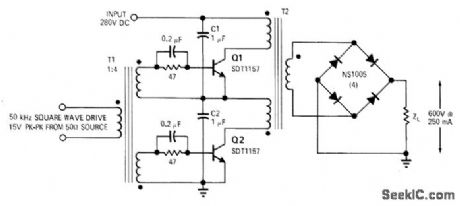
Cascode push-pull transistor switch conversion circuit uses low-voltage transistors and provides automatic equalization of transistor storage time. Drive-signal input to cascode push-pull switch is symmetrical 50-kHz 15 V P-P square wavefrom 50-ohm source. Q1 and Q2 each see only haff of DC source voltage because C1 and C2, in series across 280-V input, charge to 140 V each. Circuit is adaptable to wide range of output voltages and currents because identical units can be connected in series or parallel to obtain desired rating.—L. G.Wright and W. E. Milberger, HV Building Block Uses Series Transistor Switches, EDN Magazine, Feb. 15, 1971, p 39-40. (View)
View full Circuit Diagram | Comments | Reading(1051)
Basic_tuned_circuit
Published:2009/7/24 13:40:00 Author:Jessie
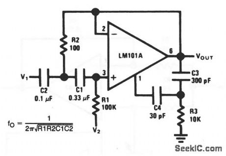
This circuit uses an LM101A to form a single-stage tuned circuit. The output frequency is determined by the values of R1, R2, C1, and C2, as shown by the equation. National Semiconductor, Linear Applications Handbook, 1991, p. 95. (View)
View full Circuit Diagram | Comments | Reading(669)
Two_stage_tuned_circuit
Published:2009/7/24 13:39:00 Author:Jessie
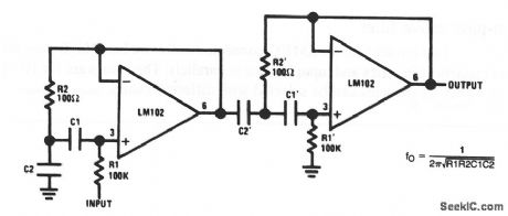
This circuit uses two LM102s to fonn a two-stage tuned circuit. National Semiconductor, Linear Applications Handbook, 1991, p. 95. (View)
View full Circuit Diagram | Comments | Reading(570)
Easily_tuned_notch_filter
Published:2009/7/24 13:39:00 Author:Jessie
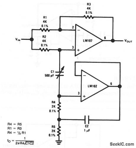
This circuit uses two LM107s to form a tunable notch filter. The notch frequency is set by adjustment of C1. The frequency range is determined by the values of R4,C1, and C2, as shown by the equation. National Semiconductor, Linear Applications Handbook, 1991, p. 95. (View)
View full Circuit Diagram | Comments | Reading(1163)
The switch circuit of light remote control lamp(1)
Published:2011/6/30 21:46:00 Author:zj | Keyword: switch circuit, light remote control lamp(1), 9013
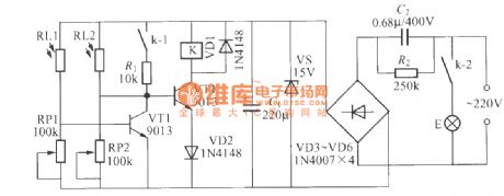
As the diagram shows,it is a switch circuit of light remote control lamp. The remote control can be electric torch or toy laser pointer. Both RL1 and RL2 use MG45 photoresistor.It requires that multiples between the light resistance and the dark resistance are the more the better.You should add shading tubes for them so as to eliminate the interference of environment light when producing. K should use the 12V work voltage. There are two small electromagnetic relays with conversion contacts,like JRX_13F,DC12V etc. (View)
View full Circuit Diagram | Comments | Reading(749)
Adjustable_Q_notch_filter
Published:2009/7/24 13:37:00 Author:Jessie
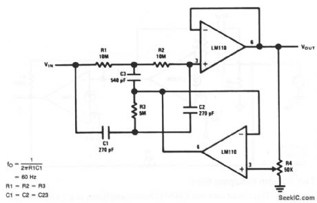
This circuit uses two LM100s to form a 60-Hz notch filter with adjustable Q(set by adjustment of R4). Other frequencies can be selected using the equation. National Semiconductor, Linear Applications Handbook, 1991, p. 94. (View)
View full Circuit Diagram | Comments | Reading(4054)
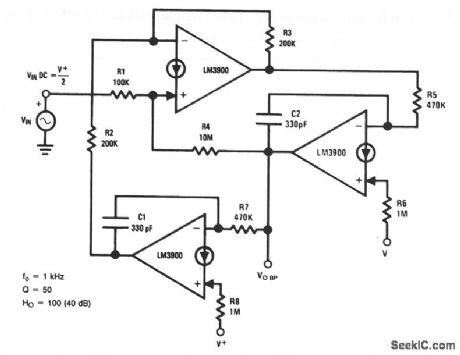
Bi_quad_RC_active_bandpass_filter
Published:2009/7/24 13:36:00 Author:Jessie
This circuit uses three LM3900 Norton amplifiers as a 1-kHz bandpass filter with a Q of 50, and a gain of 100 (40 dB). National Semiconductor, Linear Applications Handbook, 1991, p. 230. (View)
View full Circuit Diagram | Comments | Reading(883)
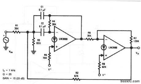
Two_op_amp_bandpass_filter
Published:2009/7/24 13:36:00 Author:Jessie
This circuit uses two LM3900 Norton amplifiers as a 1-kHz bandpass filter with a Q of 25, and a gain of 15 (23 dB). National Semiconductor, Linear Applications Handbook, 1991, p. 229. (View)
View full Circuit Diagram | Comments | Reading(1701)
One_op_amp_bandpass_filter
Published:2009/7/24 13:35:00 Author:Jessie
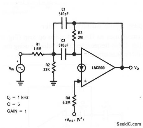
This circuit uses an LM3900 Norton amplifier as a 1-kHz bandpass filter with a Q of 5 and unity gain. National Semiconductor, Linear Applications Handbook, 1991, p. 228. (View)
View full Circuit Diagram | Comments | Reading(2365)
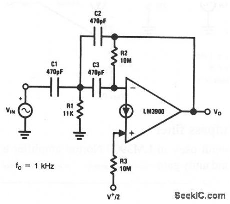
Low_pass_active_filter_with_Norton_amplifier
Published:2009/7/24 13:34:00 Author:Jessie
This circuit uses an LM3900 Norton amplifier as a 1-kHz low-pass filter. National Semiconductor, Linear Applications Handbook, 1991, p. 227. (View)
View full Circuit Diagram | Comments | Reading(1037)
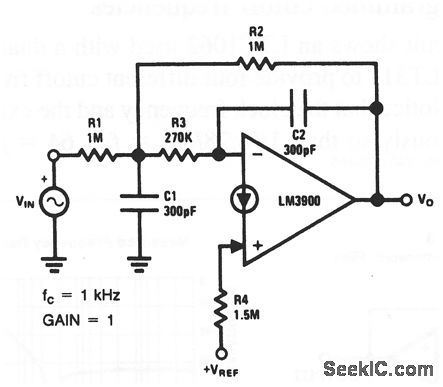
High_pass_active_filter_with_Norton_amplifier
Published:2009/7/24 13:33:00 Author:Jessie
This circuit uses an LM3900 Norton amplifier as a 1-kHz high-pass filter. National Semiconductor, Linear Applications Handbook, 1991, p. 227. (View)
View full Circuit Diagram | Comments | Reading(767)
100_kHz_high_pass_2_pole_Butterworth_filter
Published:2009/7/24 13:32:00 Author:Jessie
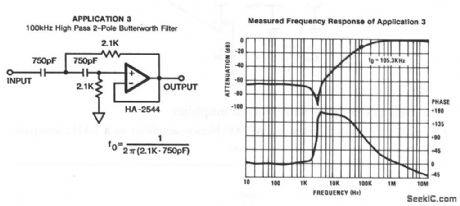
This circuit uses an HA-2544 video op amp (Fig. 3-29) to form an active 100-kHz filter. Other frequencies can be selected using the equation. Figure 7-26B shows the filter characteristics. Harris Semiconductor, Linear & Telecom ICs, 1991, p. 3-312. (View)
View full Circuit Diagram | Comments | Reading(601)
IC_filter_with_programmed_cutoff_frequencies
Published:2009/7/24 13:31:00 Author:Jessie
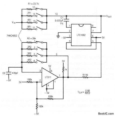
This circuit shows an LTC1062 used with a dual four-channel MUX (74HC4052) and an LT311 to provide four different cutoff frequencies (500, 250, 125, and 62.5 Hz). Notice that the clock frequency and the external R×C product are varied simultaneously so that: 1/(6.28RC) =fc/1.64=fclock/1.64. Linear Technology Corporation, Linear Applications Handbook, 1992, p. AN24-8. (View)
View full Circuit Diagram | Comments | Reading(924)
IC_filter_operated(from_±15_V)supplies
Published:2009/7/24 13:29:00 Author:Jessie
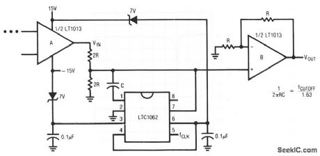
This circuit shows an LTC1062 interfaced with an LT1013 op amp and operated from ±15-V supplies.The desired cutoff frequency is determined by the equation shown. A typical dc output is 300 mV. Linear Technology Corporation, Linear Applications Handbook, 1992, p. AN24-7. (View)
View full Circuit Diagram | Comments | Reading(511)
Full_duplex_300_baud_modem_filter
Published:2009/7/24 14:03:00 Author:Jessie
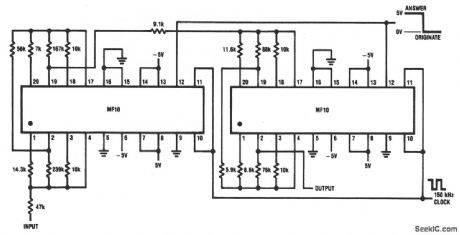
This circuit is an 8th-order 1-dB ripple Chebyshev bandpass, which functions as both an 1170-Hz originate filter, and a 2125-Hz answer filter. Only one clock is required, and overall gain is 22 dB. National Semiconductor, Linear Applications Handbook, 1991, p. 912. (View)
View full Circuit Diagram | Comments | Reading(697)
| Pages:1226/2234 At 2012211222122312241225122612271228122912301231123212331234123512361237123812391240Under 20 |
Circuit Categories
power supply circuit
Amplifier Circuit
Basic Circuit
LED and Light Circuit
Sensor Circuit
Signal Processing
Electrical Equipment Circuit
Control Circuit
Remote Control Circuit
A/D-D/A Converter Circuit
Audio Circuit
Measuring and Test Circuit
Communication Circuit
Computer-Related Circuit
555 Circuit
Automotive Circuit
Repairing Circuit