
Circuit Diagram
Index 1225
Low_pass_active_filter
Published:2009/7/24 13:44:00 Author:Jessie
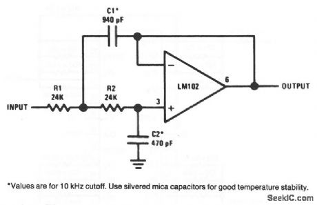
This circuit uses an LM102 connected to form a basic low-pass filter (input capacitors in parallel and input resistors in series). The values are for a 10-kHz cutoff. Other frequencies can be selected with different values. National Semiconductor, Linear Applications Handbook, 1991, p. 98. (View)
View full Circuit Diagram | Comments | Reading(1145)
High_pass_active_filter
Published:2009/7/24 13:41:00 Author:Jessie
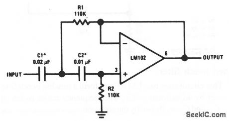
This circuit uses an LM102 connected to form a basic high-pass filter (input capacitors in series and input resistor in parallel). The values are for 100-Hz cutoff. Other frequencies can be selected with different values. National Semiconductor, Linear Applications Handbook, 1991, p. 98. (View)
View full Circuit Diagram | Comments | Reading(1847)
15_V_TO_-24_V
Published:2009/6/30 2:36:00 Author:May
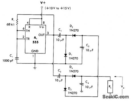
Voltage doubler is used in combination with 555 astable MVBR and two peak-to-peak detectors to give high negative voltages from positive voltage source. Load current capability is about 10 mA. Output drops to about -14.5 V when using supply of +10 V.—W. G. Jung, IC Timer Cookbook, Howard W.Sams, Indianapolis, IN, 1977, p 197-201. (View)
View full Circuit Diagram | Comments | Reading(927)
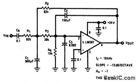
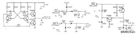
SCRATCH_FILTER_USING_LM387
Published:2009/6/30 2:36:00 Author:May
View full Circuit Diagram | Comments | Reading(719)
20_kHz_BANDPASS_ACTIVE_FILTER_
Published:2009/6/30 2:35:00 Author:May
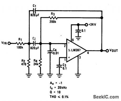
View full Circuit Diagram | Comments | Reading(648)
0_TO_-10_V_FROM__12_V
Published:2009/6/30 2:35:00 Author:May


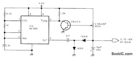
Variable-output converter using NE555 timer delivers negative output votage required by some interface devices and D/A converters used with microprocessors.—S. Ciarcia,Build a 5 W DC to DC Converter, BYTE,Oct,1978、p 22, 24, 26, 28, and 30-31. (View)
View full Circuit Diagram | Comments | Reading(1067)
RUMBLE_FILTER_USING_LM387
Published:2009/6/30 2:34:00 Author:May
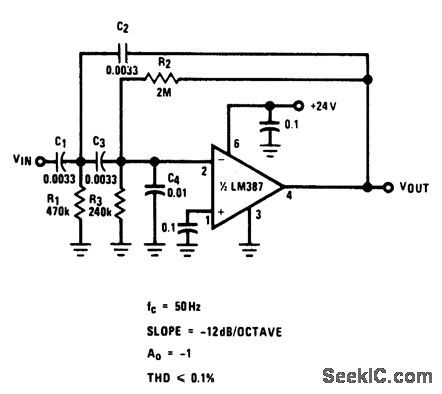
View full Circuit Diagram | Comments | Reading(762)
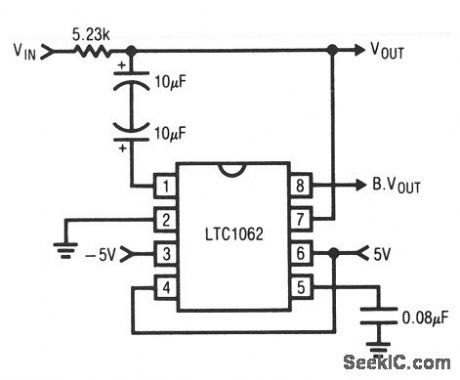
High_input_voltage_IC_filter
Published:2009/7/24 13:27:00 Author:Jessie
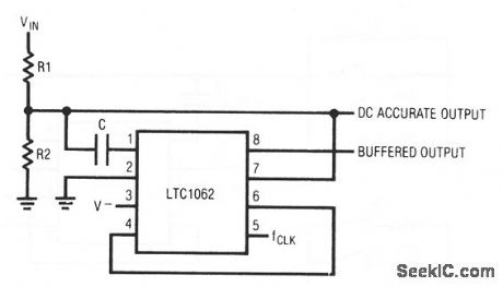

This circuit shows how an LTC1062 can be connected to accommodate high input voltages outside the normal input common-mode range. The dc gain of the low-pass filter is: R2/(R1 + R2). For maximum passband flatness, the paralleled combination of R1/R2 should be chosen as:
R1/R2≥ 5 kΩ. Notice that there is no need for an external op amp to buffer the divided-down input voltage. The internal buffer input (pin 7) performs this function. Linear Technology Corporation, Linear Applications Handbook, 1992, p. AN24-7.
(View)
View full Circuit Diagram | Comments | Reading(541)
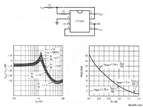
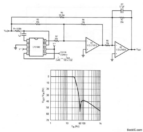
Clock_tunable_notch_filter
Published:2009/7/24 13:17:00 Author:Jessie
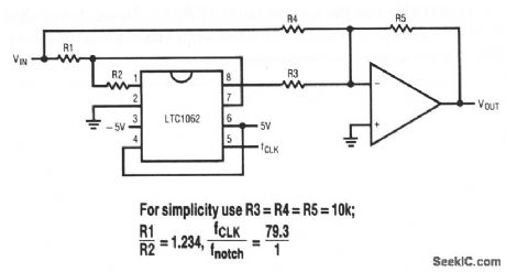
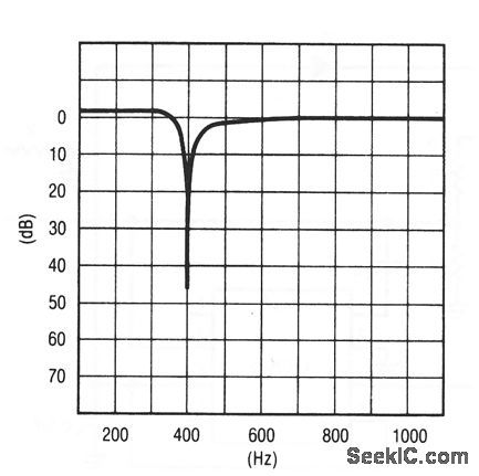
This circuit shows an LTC1062 and an op amp (such as an LT1056) connected to form a notch filter. Figure 7-22B shows the frequency response for a 400-Hz notch filter that uses the following values and equations: R3=R4=R5=10 kΩ, R1/R2=1.234Ω, fCLK/fnotch=79.3/1. Linear Technology Corporation, Linear Applications Handbook, 1990, p. AN24-6. (View)
View full Circuit Diagram | Comments | Reading(776)
_MULTIPLE_FEEDBACK__BANDPASS_FILTER(10_kHz)
Published:2009/6/30 2:32:00 Author:May
View full Circuit Diagram | Comments | Reading(699)
REGULATED__900_V_FROM__6_V
Published:2009/6/30 2:32:00 Author:May

CA3094 programmable opamp is connected as oscillator for driving step-up transformer that develops suit. able high voltage for rectification in diode network. Sample of +900 V regulated output is fed to CA3080A variable opamp through 198-meg ohm resistor of voltage divider to control pulse repetition rate of oscillator. Magnitude of regulated output is controlled by pot R. Regulation is within 1% for loads of 5 to 26μA. DC-to-DC conversion efficiency is about 50%.— Circuit Ideas for RCA Linear ICs, RCA Solid State Division, Somerville, NJ, 1977, p 19. (View)
View full Circuit Diagram | Comments | Reading(1045)
Selective_clock_sweepable_bandpass_filter
Published:2009/7/24 13:15:00 Author:Jessie
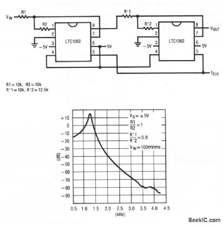
This circuit shows two LTC1062s connected to form a clock-sweepable bandpass filter. Figure 7-21B shows the frequency response for the values given in Fig. 7-21 A. Linear Technology Corporation, Linear Applications Handbook, 1990, p. AN24-5. (View)
View full Circuit Diagram | Comments | Reading(612)
TRANSFORMERLESS_POSITIVE_TO_NEGATIVE
Published:2009/6/30 2:30:00 Author:May
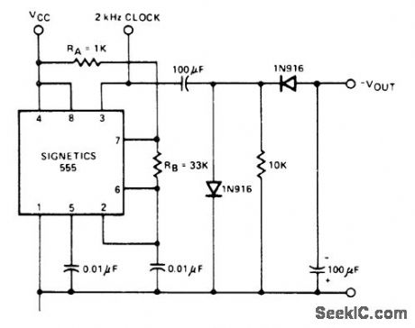
Used to derive negative supply voltage from positive supply voltage, while at same time generating 2-kHz dock signal, Negative output voltage tracks DC input voltage linearly, but magnitude is about 3 V lower. Circuit does not provide regulation.— Signetics Analog Data Manual, Signetics, Sunnyvale, CA, 1977, p 729. (View)
View full Circuit Diagram | Comments | Reading(1136)
±15_V_FROM__5_V
Published:2009/6/30 2:30:00 Author:May
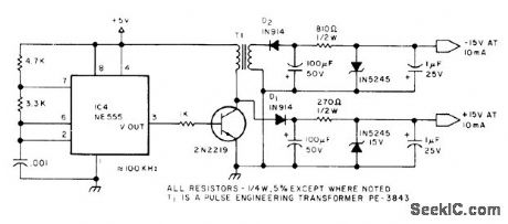
Provides positive and negative higher voltages required by some interface devices used with microprocessors. NE555 timer is connected as 100-kHz oscillator that switches transistor on and off, inducing current in primary of T1. High-voltage spike reflected back to collector of transistor by pulse transformer is routed through D1 to filter-regulator for providing positive output.—S. Ciarda, Build a 5 W DC to DC Convener, BYTE, Oct. 1978 p 22, 24,26,28, and 30-31. (View)
View full Circuit Diagram | Comments | Reading(2359)
Clock_sweepable_pseudo_bandpass_notch_filter
Published:2009/7/24 13:14:00 Author:Jessie
This circuit shows an LTC1062 connected as a simple clock-sweepable bandpass/notch filter. Figure 7-20B shows the frequency response for a clock frequency of 100 kHz and the various ratios of R1/R2. Figure 7-20C shows the variation of peak gain (Hop) and peak frequency (fp) versus different values of the R1/R2 ratio. Linear Technology Corporation, Linear Applications Handbook, 1990, p. AN24-4,-5. (View)
View full Circuit Diagram | Comments | Reading(568)
Simple_5_Hz_filter_that_uses_back_to_back_capacitors
Published:2009/7/24 13:13:00 Author:Jessie
This circuit shows an LTC1062 connected with solid-tantalum capacitors to form a 5-Hz low-pass filter. Notice that no external clock is required. Linear Technology Corporation, Linear Applications Handbook, 1990, p. AN20-11. (View)
View full Circuit Diagram | Comments | Reading(816)
POLARITY_REVERsER
Published:2009/6/30 2:28:00 Author:May
Simple RC osdllator operating at about 1200 Hz can be used with choice of rectifier circuits to provide negative or positive voltages equal to or higher than DC supply, without use of transformer. Output transistors connect Ioad altemately to positive supply and to ground for high operating efficiency. Two-diode voltage doubler with connection to 12-V supply gives positive output.Other diode rectifier cilcuit doubles oscillatol output and gives negative supply. Negative doubler uses switching transistors. All three rectifier circuits provide common ground from supply to output.—J. M. Pike, Negative and High Voltagesfrom a Positive Supply, QST, Jan.1974, p 23-25 (View)
View full Circuit Diagram | Comments | Reading(0)
Extended_notch_filter
Published:2009/7/24 13:12:00 Author:Jessie
This circuit is similar to that of Fig. 7-17, but uses two sections of an LT1013 following the LTC1062. Figure 7-18B shows the frequency response for a 60-Hz notch filter that uses the values and equations of Fig. 7-18A. Linear Technology Corporation, Linear Applications Handbook, 1990, p. AN20-10,-11. (View)
View full Circuit Diagram | Comments | Reading(564)
IC_notch_filter
Published:2009/7/24 13:10:00 Author:Jessie
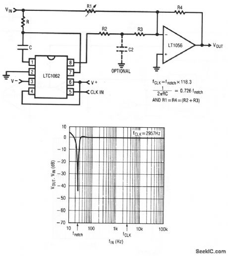
This circuit shows an LTC1062 and an LT1056 connected to form a notch filter. Figure 7-17B shows the frequency response for a 25-Hz notch filter using values based on the equations of Fig. 7-17A. The optional R2/C2 at the LTC1062 output is used to minimize clock feedthrough. The 1/(6.28R2C2) value should be 12 to 15 times that of the notch frequency. Linear Technology Corporation, Linear Applications Handbook, 1990, p. AN20-9, -10. (View)
View full Circuit Diagram | Comments | Reading(1072)
HARMONIC_DISTORTION_METER
Published:2009/6/30 2:27:00 Author:May
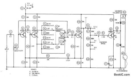
Used to measure total harmonic distortion of audio amplifier、component、or network.Pure sine-wavesignal is applied to devlee under test, and output of device is fed to AF input of distortion meter. After setting S2 to appropriate frequency range, close S1, set S3 at A, set S4 at appropriate voltage range, and adjust R1 for fullscale meter deflection. Record this voltage as E1. Set S3 to B, tune C3 for null, then set S4 to successively lower ranges for accurate reading of voltage at null. Record residual null voltage as E2. Percentage distortion is then 100E2/ E1.-R. P. Tumer, FET Circuits, Howard W.Sams, Indianapolis, IN, 1977, 2nd Ed., p 147-150. (View)
View full Circuit Diagram | Comments | Reading(3122)
| Pages:1225/2234 At 2012211222122312241225122612271228122912301231123212331234123512361237123812391240Under 20 |
Circuit Categories
power supply circuit
Amplifier Circuit
Basic Circuit
LED and Light Circuit
Sensor Circuit
Signal Processing
Electrical Equipment Circuit
Control Circuit
Remote Control Circuit
A/D-D/A Converter Circuit
Audio Circuit
Measuring and Test Circuit
Communication Circuit
Computer-Related Circuit
555 Circuit
Automotive Circuit
Repairing Circuit