
Circuit Diagram
Index 1227
4th_order_1_kHz_Butterworth_switched_filter
Published:2009/7/24 14:02:00 Author:Jessie
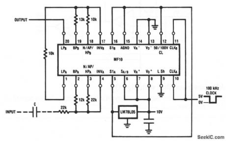
Only six resistors are required for this low-pass filter. However, a 100-kHz clock is required. National Semiconductor, Linear Applications Handbook, 1991, p. 910. (View)
View full Circuit Diagram | Comments | Reading(615)
Universal_state_variable_filter
Published:2009/7/24 14:01:00 Author:Jessie
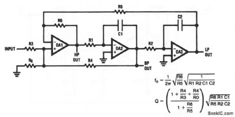
This circuit uses three op amps to form a universal state-variable filter. Compare this circuit and equations to that of Fig. 7-6. National Semiconductor, Linear Applications Handbook, 1991, p. 903. (View)
View full Circuit Diagram | Comments | Reading(2474)
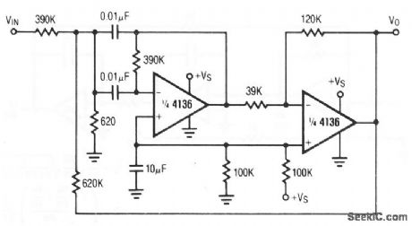
1_kHz_bandpass_filter_with_high_Q
Published:2009/7/24 14:00:00 Author:Jessie
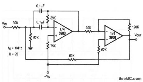
This circuit uses two sections of a 3900 op amp to form a high-Q (Q=25) bandpass filter. Raytheon Linear Integrated Circuts, 1989, p. 4.274. (View)
View full Circuit Diagram | Comments | Reading(1704)
OUAD_GAIN_CONTROL
Published:2009/6/30 2:20:00 Author:May

Combination of National AM97C11 quad FET and LM324 quad opamp gives tracking gain control having 40-dB range. Bandwidth is 10 kHz minimum, and S/N ratio is better than 70 dB for 4.3-VRMS maximum output. Temperature sensitivity of FET can be reduced by using silicon resistor for opamp feedback resistor R1.- FET Databook, National Semiconductor, Santa Clara, CA, 1977, p 6-39-6-46. (View)
View full Circuit Diagram | Comments | Reading(923)
NOISELESS_AUDIO_SWITCH
Published:2009/6/30 2:17:00 Author:May
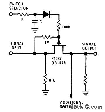
Deglitched current-mode switch using JFET can be placed directly on printefficircuit board instead of front panel, to minimize hum pickup and crosstalk.JFET allows transition time of drive to be adjusted with series resistor R and shunt capacitor C to provide noiseless switching of AF signals.Diode type is not critical. Any number of switches can be ganged.- Audio Handbook, National Semiconductor, Santa Clara, CA, 1977, p2-62. (View)
View full Circuit Diagram | Comments | Reading(3165)
1_kHz_bandpass_filter
Published:2009/7/24 13:59:00 Author:Jessie
This circuit uses two sections of a 4136 op amp to form a bandpass filter. Raytheon Linear Integrated Circuts, 1989, p. 4-175. (View)
View full Circuit Diagram | Comments | Reading(917)
Dc_accurate_low_pass_bandbass_filter
Published:2009/7/24 13:58:00 Author:Jessie
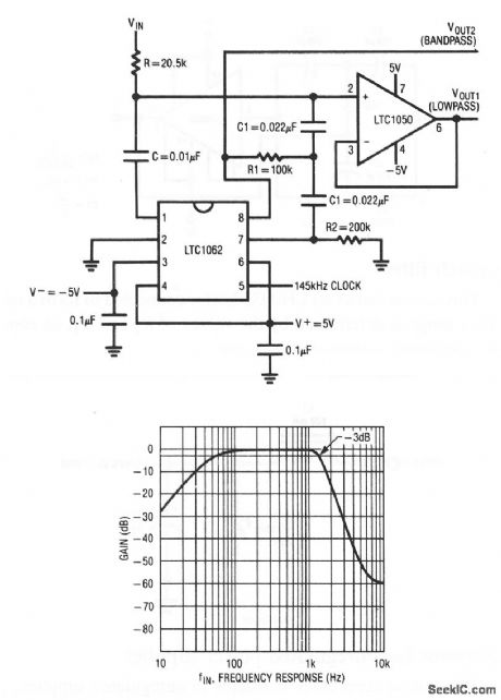
This circuit uses an LTC1050 and LTC1062 to form a filter that extracts ac information from a dc +ac signal. Figure 7-48B shows the bandpass-filter output characteristics. Linear Technology, Linear Appications Handbook, 1990, p. DN9-2. (View)
View full Circuit Diagram | Comments | Reading(605)
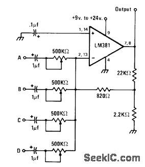
FOUR_CHANNEL_MIXER_1
Published:2009/6/30 2:16:00 Author:May
Combines AF signals from one to four sources into single audio signal for input of LM381 opamp that serves also as preamp. Shield mixer circuit and use shielded cable for all input leads to avoid pickup of 60-Hz field by high-gain opamp. Increasing supply voltagefrom minimum of 9V boosts outputsig-nal voltage.-J. A Sandier, 9 Easyto Build Projects under $9, Modern Electronics, July 1978, p 53-56. (View)
View full Circuit Diagram | Comments | Reading(1982)
Spike_suppressor_for_unregulated_power_supplies
Published:2009/7/24 13:56:00 Author:Jessie
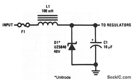
This circuit suppresses transients in unregulated supplies. Zener D1 clamps the input voltage to the regulator, and L1 limits the current through D1 during the transient. This circuit will clamp 70-V 4-ms transients. The value of L1=dVdt/I, where dV is the voltage by which the input transient exceeds the breakdown voltage of D1, dt is the duration of the transient, and I is the peak current of D1. National Semiconductor, Linear Applications Handbook, 1991, p. 47. (View)
View full Circuit Diagram | Comments | Reading(828)
45_MHz_notch_filter
Published:2009/7/24 13:54:00 Author:Jessie
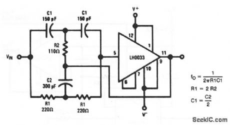
This circuit shows an LH0033 buffer connected to form a notch filter. The frequency range is determined by the values of R1 and C1, as shown by the equation. National Semiconductor, Linear Applications Handbook, 1991, p. 161. (View)
View full Circuit Diagram | Comments | Reading(660)
5_V_TO_400_V
Published:2009/6/30 2:16:00 Author:May
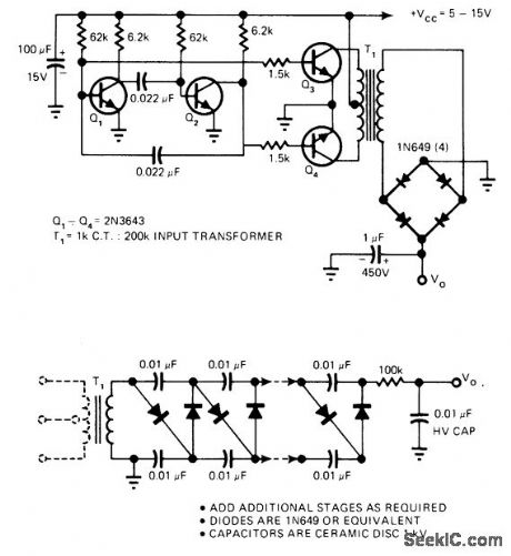
Astable MVBR operating at 2.174 kHz for values shown drives push-pull transistor pair feeding primary of audio input transformer T1. Secondary voltage is rectified by diode bridge to provide DC output voltage ranging from 100 to 400 V depending on load resistance and exact value of supply voltage VCC.Bridge rectifier can be replaced by 40-stage multiplier as shown in lower diagram, to give 10-kVDC output.—A. M. Hudor, Jr., Power Converter Uses Low-Cost Audio Transformer, EDN Magazine, April 20, 1977, p 139. (View)
View full Circuit Diagram | Comments | Reading(1344)
Fed_forward_low_pass_filter
Published:2009/7/24 13:53:00 Author:Jessie
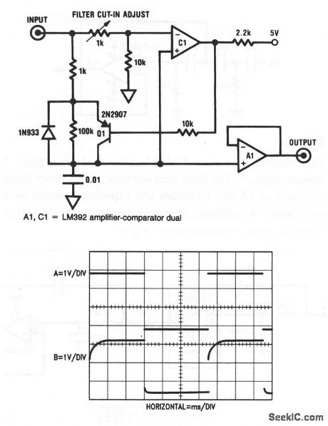
This circuit allows a signal to be rapidly acquired to final value, but it provides a long filtering constant. Such a characteristic is useful in multiplexed data-acquisition systems, and has been used in electronic infant-weighing scales, where fast, stable readings of weight are needed (in spite of motion on the scale platform). The point at which the filter switches from a short to a long time constant is set by the 1-kΩ pot. Normally, this is adjusted so that switching-occurs at 90% to 98% of final value. However, the waveforms shown in Fig. 7-45B were obtained at a 70% trip point to show circuit operation. National Semiconductor, Linear Applications Handbook, 1991, p. 835. (View)
View full Circuit Diagram | Comments | Reading(657)
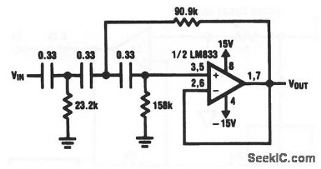
Ultrasonic_filter
Published:2009/7/24 13:51:00 Author:Jessie
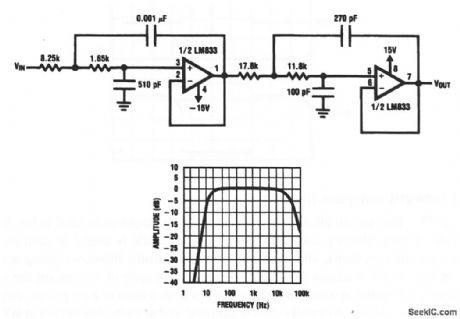
This circuit shows both sections of an LM833 that is connected as a filter to reject undesired ultrasonic signals. The filter characteristic is 4th-order Bessel with the -3-dB frequency at about 40 kHz. Resistors and capacitors should be 1%-tolerance components. This circuit can be cascaded with that of Fig. 7-43 (with the low-pass preceding the high-pass) to produce a response such as shown in Fig. 7-44B. National Semiconductor, Linear Applications Handbook, 1991, p. 944,945. (View)
View full Circuit Diagram | Comments | Reading(2994)
Infrasonic_filter
Published:2009/7/24 13:51:00 Author:Jessie
This circuit shows an LM833 connected as a filter for rejecting undesired infrasonic signals. The filter characteristic is 3rd-order Butterworth with the -3-dB frequency at 15 Hz. Resistors and capacitors should be 1%-tolerance components (although 5%-tolerance components can be substituted in less critical applications). National Semiconductor, Linear Applications Handbook, 1991, p. 944. (View)
View full Circuit Diagram | Comments | Reading(1011)
Wideband_two_pole_high_pass_filter
Published:2009/7/24 13:50:00 Author:Jessie
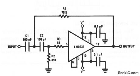
This circuit shows an LH0033 buffer connected to form a basic two-pole high-pass filter with a 10-Hz cutoff frequency. A low-pass filter with the same frequency can be obtained by interchanging R1, R2, C1, and C2. National Semiconductor, Linear Applications Handbook, 1991, p. 542. (View)
View full Circuit Diagram | Comments | Reading(1878)
_12V_TO__8_V
Published:2009/6/30 2:14:00 Author:May
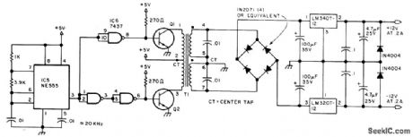
NE555 timer connected as 20-kHz oscillator drives pair of D44H4 transistors through 7437 quad two-input NAND buffer to produce full 200 mA of regulated output for each polarity. Circuit uses push-pull inverter technique to generate AC for driving transformer constructed by rewinding 88-mH toroid to have 40 turns No, 20 center-tapped for primary and 350 turns No. 26 center-tapped for secondary.—S, Ciarcia, Build a 5 W DC to DC Converter, BYTE, Oct. 1978, p 22, 24 26, 28, and 30-31. (View)
View full Circuit Diagram | Comments | Reading(2830)
EQUALIZER
Published:2009/6/30 2:14:00 Author:May
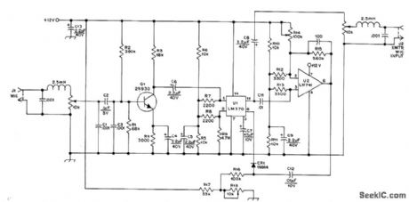
Designed for use between input jack and microphone of amateur transmitter, to keep bandpass response between limits of about 200 and 3100Hz. Circuit also provides measure of volume compression, improving transmitter efficiency. Construction and ad justment details stress importance of eliminating ground loops and RF feedback. Un is voltage-controlled amplifier in feedback loop, with 741 opamp U2 as compression detector. U2 is biased so output is almost at ground, and no feedback voltage is applied until input to U2 exceeds 0.9 V. U: thus operates in linear mode at maximum gain until output voltage exceeds 0.9 V, when voltage is applied to UI and gain of IC is reduced.-R. Tauber, The Equalizer, QST, March 1977, p 18-20. (View)
View full Circuit Diagram | Comments | Reading(2681)
TONE_DRIVEN_RELAY
Published:2009/6/30 2:13:00 Author:May
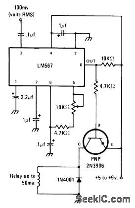
LM567 tone decoder will respond to frequency between 700 and 1500 Hz, determined by setting of 10K pot.When input of 100 mVRMS at preset frequency arrives, output of IC goes low and energizes relay through transistor. Tone can be obtained from audio oscillator or telephone Touch-Tone pad. Relay contacts can be used to turn desired device on or off.-J. A. Sandier, 9 Easy to Build Projects under $9, Modern Electronics, July 1978, p 53-56. (View)
View full Circuit Diagram | Comments | Reading(1642)
VOLTAGE_CONTROLLED_ATTENUATOR
Published:2009/6/30 2:12:00 Author:May
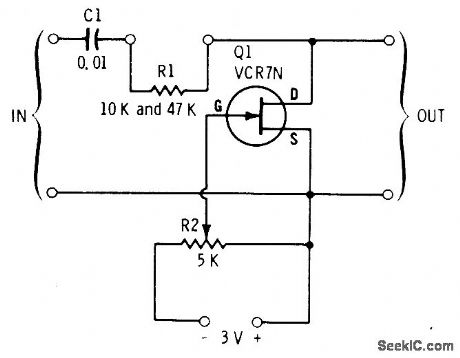
Used to control low-level audio signals with variable DC voltage of ±3V. Control pot can be remotely located. Highest possible output is equal to input level, occurring when gate bias is set close to pinchoff value. Output is minimum when gate bias is zero.-E, M. Noll, FET Principles, Experiments, and Projects, Howard W. Sams, Indianapolis, IN, 2nd Ed., 1975, p 258-260. (View)
View full Circuit Diagram | Comments | Reading(0)
6_V_TO_±15_V
Published:2009/6/30 2:12:00 Author:May
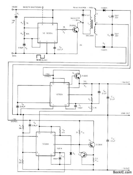
Combination of 555 timer and two NE550 voltage regulators provides voltage mu Itiplication along with regulation of independent DC outputs. Selected oscillator frequency of 17 kHz optimizes performance of transformer. Can be used to power opamps from either TTL supplies or 6-V batteries. Line and load regulationare 0.1 %, while power efficiency at full load of 100 mA is better than 75%.—R.Solomon and R. Broadway, DC-to-DC Converter Uses IC Timer, EDN Magazine, Sept. 5, 1973, p 87, 89, and 91. (View)
View full Circuit Diagram | Comments | Reading(1443)
| Pages:1227/2234 At 2012211222122312241225122612271228122912301231123212331234123512361237123812391240Under 20 |
Circuit Categories
power supply circuit
Amplifier Circuit
Basic Circuit
LED and Light Circuit
Sensor Circuit
Signal Processing
Electrical Equipment Circuit
Control Circuit
Remote Control Circuit
A/D-D/A Converter Circuit
Audio Circuit
Measuring and Test Circuit
Communication Circuit
Computer-Related Circuit
555 Circuit
Automotive Circuit
Repairing Circuit