
Circuit Diagram
Index 1241
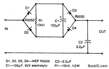
LOW_PASS_FILTER
Published:2009/6/29 21:40:00 Author:May
Circuit Notes
This nonlinear, passive filter circuit rejects ripple (or unwanted but fairly steady voltage) without appreciably affecting the rise time of a signal. The circuit works best when the signal level is considerably lower than the unwanted ripple, provided the ripple level is fairly constant. The circuit has characteristics similar to two peakdetecting sample-and-hold circuits in tandem with a voltage averager. (View)
View full Circuit Diagram | Comments | Reading(131)
Multiplexed_cable_driver_8_channel
Published:2009/7/24 21:34:00 Author:Jessie
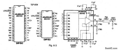
Figure 6-3 shows a multiplexer/amplifier MAX440 connected to provide 8 channels of video signal to a single cable. Unity-gain bandwidth is 160 MHz, 6-dB-gain bandwidth is 110 MHz, channel-switch time is 15 ns, slew rate is 370 V/μs, and on/off input capacitance is 4 pF. MAXIM NEW RELEASES DATA BOOK, 1993, P. 3-15. (View)
View full Circuit Diagram | Comments | Reading(644)
Remote Multi Point Control Switch Circuit
Published:2011/7/21 18:43:00 Author:Joyce | Keyword: Remote, Multi Point , Control , Switch
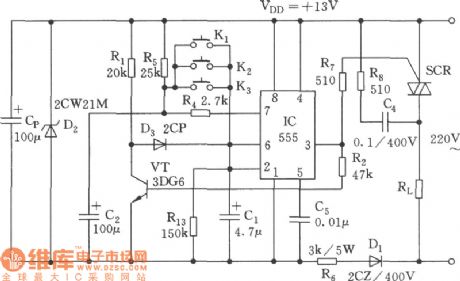
As shown in the figure, the switch circuit includes a depressurization and rectification circuit, a bistable trigger circuit and a silicon controlled control circuit. It will remote control the start up and close down of electric equipment .The depressurization and rectification circuit provides the controller with + 13 V dc voltage. 555, R5, R4, R13, C1, C2, and some other components constitute the bistable trigger circuit. At the moment it is switched on, because the voltage on C1 will not change suddenly, 555 will set, and C2 will be charged to 12V through R5. At this time, if one presses K1 (K2 or Ks), C1 will soon be charged to2/3 VDD = 8 V, and 555 will reset, feet 3 will show a low level, and SCR will cut off. At the same time, VT will cut off; feet 6 of 555 will display a high level to keep 555 in a stable state of reset. (View)
View full Circuit Diagram | Comments | Reading(904)
Inverting_amplifier
Published:2009/7/24 21:32:00 Author:Jessie
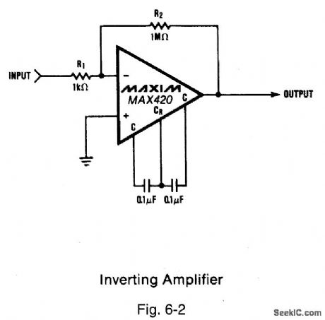
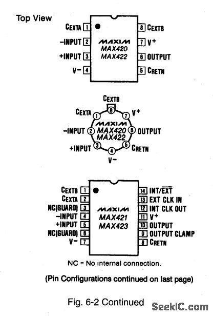
Figure 6-2 shows a chopper-stabilized MAX420 connected as an inverting amplifier. The offset voltage is 5 μV maximum; the input voltage range is + 12 V to -15 V with ±15-V supplies; the input noise is 0.3 μVp-p from dc to 1 Hz; the gain, CMRR, and PSRR are all 120 dB; the maximum supply current is 0.5 mA; and the input bias current is 30 pA. MaxnIM HIGH-RELIABILITY DATA BOOK, 1993, P. 3-11. (View)
View full Circuit Diagram | Comments | Reading(0)
Threshold_detector_for_rphotodiodes
Published:2009/7/24 21:31:00 Author:Jessie
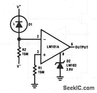
This circuit converts small input currents produced by D1 into levels suitable to drive DTL/TTL loads. Different values of R1/R2 can be selected to set different on/off levels. (View)
View full Circuit Diagram | Comments | Reading(647)
VARIABLE_BANDWIDTH_BANDPASS_ACTIVE_FILTER
Published:2009/6/29 21:36:00 Author:May

Circuit Notes
This circuit has adjustable bandwidthwith values for a center frequency of about 800 Hz. The10 K pot adjusts bandwidth from approximately ±350 Hz to ±140 Hz at 3 dB down points. (View)
View full Circuit Diagram | Comments | Reading(824)
Low_noise_instrumentation_amplifier
Published:2009/7/24 21:30:00 Author:Jessie
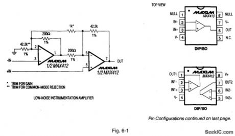

Figure 6-1 shows a low-noise instrumentation amplifier using both sections of a MAX412. Input voltage-noise density is less than 2.4 nV√Hz at 1 kHz. The output voltage swing is 7.3 Vp-p into 2 kΩ from ±5-V supplies. Supply current is 2.5 mA per amplifier, unity-gain bandwidth is 28 MHz, slew rate is 4.5 V/μs, maximum offset voltage is 250 μV, and minimum voltage gain is 115 dB. MAXIM HIGH-RELIABILITY DATA BOOK, 1993, P. 3-9. (View)
View full Circuit Diagram | Comments | Reading(0)
Voltage_comparator_with_DTL_TTL_output
Published:2009/7/24 21:30:00 Author:Jessie
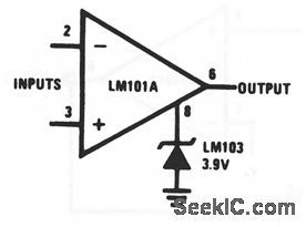
This circuit converts small differential-input signals into levels suitable to drive DTL/TTL loads. (View)
View full Circuit Diagram | Comments | Reading(743)
Multiple_aperture_window_discriminator
Published:2009/7/24 21:28:00 Author:Jessie
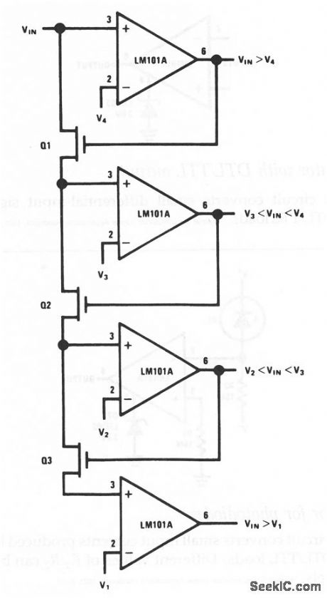
This circuit compares the input voltage with four reference voltages (V1 through V4) and produces corresponding outputs. (View)
View full Circuit Diagram | Comments | Reading(28)
33_5_V_12_V_and__18_V_from_two_to_three_cells
Published:2009/7/24 23:19:00 Author:Jessie
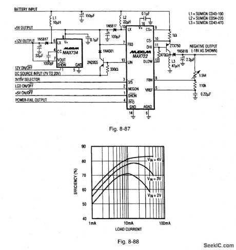
Figure 8-87 shows a MAX722 palmtop SMPS (surface-mount power supply), and a MAX734 regulator connected to provide a main 3.3-V/5-V output, a +12-V output for flash programming, and a -18-V output for LCD bias-all with a 1.8-V to 5.5-V input range. Quiescent current (when VIN = 3 V, and the 12-V line is off) is 350 μA. With a VIN of 2 V, the maximum load capability for the 5-V output is 200 mA, and the +12-V output, 40 mA. When VIN is increased to 2.5 V, the 5-V output provides 275 mA, and the +12-V output, 60 mA. Figure 8-88 shows the efficiency curves for the + 12-V output. If the main output is set at 3.3 V (pin 3 of the MAX722 high), connect the MAX734 V + pin to +12 V (instead of +5 V, as shown) to get the extra gate drive for the MAX734 MOSFET. MAXIM BATTERY MANAGEMENT CIRCUIT COLLECTION, 1994, P. 12. (View)
View full Circuit Diagram | Comments | Reading(677)
Precision_ac_to_dc_converter
Published:2009/7/24 22:59:00 Author:Jessie
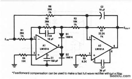
This circuit converts the half-wave rectifier or Fig. 10-39 to a full-wave rectifier. The conversion accuracy is better than 1% to above 100 kHz, with less than 1% ripple at 20 Hz. Using the values shown, the output is calibrated to read the rms value of a sine-wave input. (View)
View full Circuit Diagram | Comments | Reading(3384)
Input_signal_conditioner_for_low_voltage_ADC
Published:2009/7/24 22:08:00 Author:Jessie
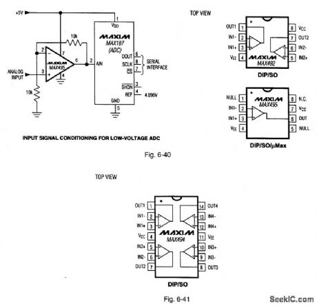
Figure 6-40 shows a MAX495 connected as an input signal conditioner for a MAX187 ADC. The MAX495 can operate from either a single supply (+2.7 V to +6 V) or split supplies (±1.35 V to ±3 V). Each op amp requires less than 150 μA supply current, but it can drive a 1-kΩ load. The input-referred voltage noise is 25 nV√Hz, the offset is 200 μV, and the gain-bandwidth is 500 kHz (see Fig. 6-41 for additional pin configurations). MAXIM NEW RELEASES DATA BOOK, 1995, P. 3-23, 3-37. (View)
View full Circuit Diagram | Comments | Reading(1004)
NICAD_CHARGER_FOR_AUTO
Published:2009/6/29 21:35:00 Author:May
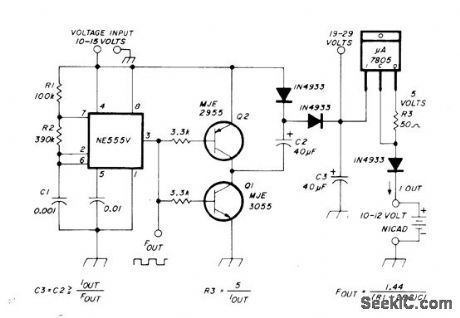
Voltage doubler provides at least 20 V from 12-V auto battery, for constant-current charging of 12-V nicads, using NE555 timer and two power transistors. Doubled voltage drives source current into three-terminal current regulator. Switching frequency of NE555 as MVBR is 1.4 kHz. Charging currentis set at 50 mA for charging ten 500-mAh nicads.-G. Hinkle, Constant-Current Battery Charger for Portable Operation, Ham Radio, April 1978, p 34-36. (View)
View full Circuit Diagram | Comments | Reading(2080)
Inductive Automatic Switch Circuit
Published:2011/7/21 18:56:00 Author:Joyce | Keyword: Inductive, Automatic , Switch
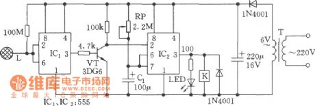
As shown in the figure, two 555s are the core of the automatic switch circuit, IC1 works as a trigger, and IC2 is used as a monostable time circuit. When the human body gets close to or touches the metal plate, IC1 will be triggered to overturn by the induction signal, so feet 3 will display a high level, and VT will be saturated and break over; IC2 will be triggered because feet 2 shows a low level (less than 1/3 VDD), turning into the state of temporary stability. Feet 3 will display a high level, K will actuate and the controlled equipment will be connected. Conversely, it will be disconnected. Timing time is: td = 1.1 RP C1, and it can be regulated by adjusting RP. (View)
View full Circuit Diagram | Comments | Reading(621)
Single_supply_differential_amplifiers
Published:2009/7/24 22:07:00 Author:Jessie
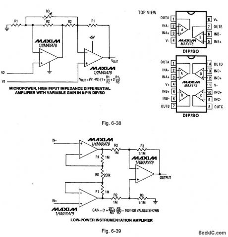
Figure 6-38 shows a MAX478 connected as a differential amplifier with variable gain. Figure 6-39 shows the MAX479 connected as a differential instrumentation amplifier. Both circuits can operate from a single supply, either 3 V or 5 V.Maximum Supply current is 17μA per op amp, the maximum offset voltage is 70 μV, maximum offset-voltage drift is 2.2 μV/℃ (0.5 μV/℃ typical) and maximum input-offset current is 250 pA. MAXIM NEW RELEASES DATA BOOK, 1994, P. 3-59, 3-69. (View)
View full Circuit Diagram | Comments | Reading(984)
Precision_high_gain_differential_amplifier_low_noise
Published:2009/7/24 22:05:00 Author:Jessie

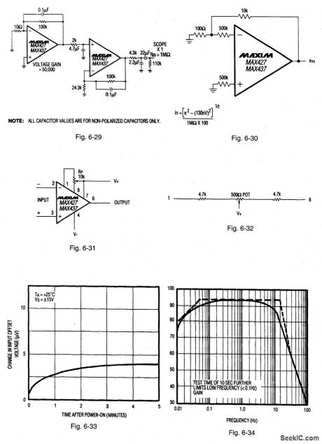
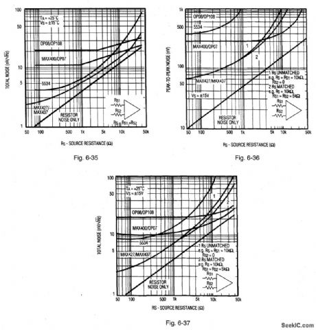
Figure 6-28 shows a MAX427 connected for differential operation. Wideband noise is 2.5 nV√Hz, offset is less than 15 μV (5-μV typical), and drift is less than 0.8 μV/℃ (0.1 μV/℃ typical). The voltage gain is 20 million when driving a 2-kΩ load to±12 V, and 12 million with a 600-Ω load to ±10 V. The MAX427 is unity-gain stable, with an 8-MHz gain-bandwidth, and a 2.5-V/μs slew rate. The decompensated MAX437 has a 60-MHz gain-bandwidth, a 15-V/μs slew rate, and is stable for closed-loop gains of five or greater. Both ICs can be operated from ±5-V supplies. Figures 6-29 and 6-30 show voltage-noise and current-noise test circuits, respectively. Figures 6-31 and 6-32 show offset-voltage adjustment circuits. Figure 6-33 shows typical offset-voltage characteristics. Figures 6-34 through 6-37 show noise characteristics. MAXIM NEW RELEASES DATA BOOK, 1994, P. 3-45. (View)
View full Circuit Diagram | Comments | Reading(1087)
Voltage_follower_with_increased_accuracy_001_μF
Published:2009/7/24 21:59:00 Author:Jessie
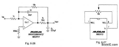
Figure 6-26 shows a voltage follower with increased accuracy (see Fig. 6-1 for pin configurations). The feedback around isolation resistor R1 increases the accuracy and the load capability. To drive capacitive loads greater than 0.01 μF, increase the value of CF. Figure 6-27 shows a null offset circuit suitable for the circuits of Figs. 6-22, 6-24, and 6-26. MAXIM NEW RELEASES DATA BOOK, 1994, P. 3-42. (View)
View full Circuit Diagram | Comments | Reading(699)
400_Hz_LOW_PASS_BUTTERWORTH_ACTIVE_FILTER
Published:2009/6/29 21:34:00 Author:May
View full Circuit Diagram | Comments | Reading(622)
NICAD_ZAPPER
Published:2009/6/29 21:33:00 Author:May
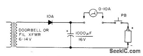
Simple circuit often restores dead or defective nicad battery by applying DC overvoltage at current up to 10 A for about 3 s. Longer treatment may overheat battery and make it explode.-Circuits, 73 Magazine, July 1977,p 35. (View)
View full Circuit Diagram | Comments | Reading(1273)
LED_TRICKLE_CHARGER
Published:2009/6/29 21:32:00 Author:May
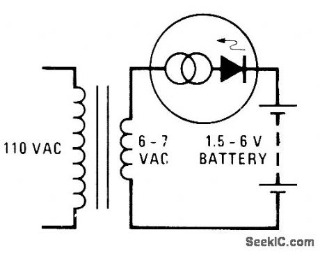
Constant-current characteristic of National NSL4944 LED is used to advantage in simple half-wave charger for batteries up to 6 V.- Linear Applications, Vol.2, National Semiconductor, Santa Clara, CA, 1976,AN-153,p 2. (View)
View full Circuit Diagram | Comments | Reading(985)
| Pages:1241/2234 At 2012411242124312441245124612471248124912501251125212531254125512561257125812591260Under 20 |
Circuit Categories
power supply circuit
Amplifier Circuit
Basic Circuit
LED and Light Circuit
Sensor Circuit
Signal Processing
Electrical Equipment Circuit
Control Circuit
Remote Control Circuit
A/D-D/A Converter Circuit
Audio Circuit
Measuring and Test Circuit
Communication Circuit
Computer-Related Circuit
555 Circuit
Automotive Circuit
Repairing Circuit