
Circuit Diagram
Index 1246
28_V_WIDEBAND_AMPLIFIER3_to_100_MHz
Published:2009/6/29 4:14:00 Author:May
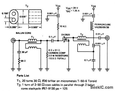
View full Circuit Diagram | Comments | Reading(688)
TWO_STAGE_60_MHz_IF_AMPLIFIER_POWER_GAIN≈80_dB_BW≈15_MHz
Published:2009/6/29 4:13:00 Author:May
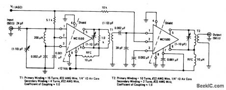
View full Circuit Diagram | Comments | Reading(608)
TWO_METER_lO_WATT_POWER_AMPLIFIER
Published:2009/6/29 4:12:00 Author:May
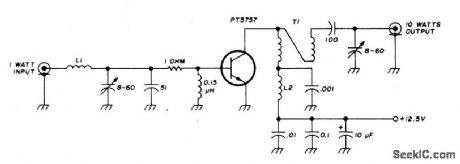
This 10-watt, 144-MHz power amplifier uses a TRW PT5757 transistor. L1 is 4 turns of no. 20 enameled, 3/32 ID; L2 is 10 turns of no. 20 enameled, 3/32 ID. Transformer T1 is a 4:1 transmission-line transformer made from a 3 length of twisted pair of no. 20 enameled wire. (View)
View full Circuit Diagram | Comments | Reading(1104)
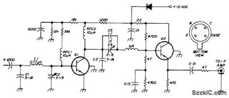
LOW_NOISE_BROADBAND_AMPLIFIER
Published:2009/6/29 4:11:00 Author:May
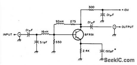
The amplifier provides 10 dB of gain from 10-600 MHz and has a 1.5-to-1 match at 50 ohms. The BFR91 has a 1.5 dB noise figures at J, 500 MHz. The circuit requires 13.5 Vdc at about 13 mA. Keep the leads on the 150 pF emitter bypass capacitor as short as possible.The 16 nH coil is 2.5 tums of #26 enamel wire on the shank of a #40 drill. The 93 nH inductor is 10 tums of the same material. (View)
View full Circuit Diagram | Comments | Reading(5450)
LOW_NOISE_30_MHz_PREAMPLIFIER
Published:2009/6/29 4:10:00 Author:May
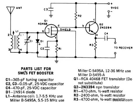
Low-noise preamplifier has a noise figure of 1.1 dB at 30 MHz and 3 dB bandwidth of 10 MHz. Gain is 19 dB. Total current drain with a +10 volt supply is 13 mA. All resistors are 1/4 watt carbon; bypass capacitors are 50-volt ceramics. (View)
View full Circuit Diagram | Comments | Reading(1259)
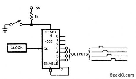
RADIO_CONTROL_RECEIVER_DECODER
Published:2009/6/29 4:03:00 Author:May
View full Circuit Diagram | Comments | Reading(1488)
LATCHING_GATES
Published:2009/6/29 4:01:00 Author:May
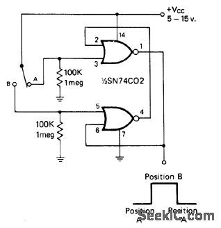
SN74C02 quad two-input NOR gate forms latching circuit in which first noise pulse produced by switch latches circuit, making it immune to contact bounce.—I. Math, Bounceless Switch, CQ, July 1976, p 50. (View)
View full Circuit Diagram | Comments | Reading(1072)
1kHz Audio Square Wave Generator Circuit
Published:2011/7/21 0:20:00 Author:Joyce | Keyword: 1kHz, Audio , Square Wave , Generator
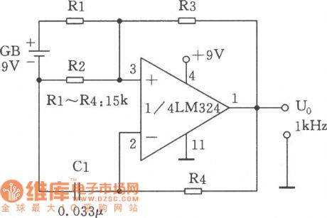
This 1 kHz audio square wave generator is mainly composed of comparator LM324 and R2, R3, R4, C1. The circuit is as shown in the figure. Reference voltage GB / 2 at the input end feet 3 of LM324 is received through bleeder circuit R1, R2. R2, R3 constitute positive feedback, while integrating circuit R4、C1 compose negative feedback .Set the value of R2,R3 to make the following formula work out: R2 / (R2 + R3) = 0.5, and repeat frequency of the square wave is: f = 1/2R4·Cl . If C1 = 0.033 pF,R4 = 15 kΩ, the value of f should be 1kHz. Changing C1 or R4 will change the oscillation frequency. (View)
View full Circuit Diagram | Comments | Reading(3587)
REMOTE_CONTROL_SERVO_SYSTEM
Published:2009/6/29 4:01:00 Author:May
View full Circuit Diagram | Comments | Reading(1104)
BOUNCE_FREE_INTERLOCKING
Published:2009/6/29 4:01:00 Author:May
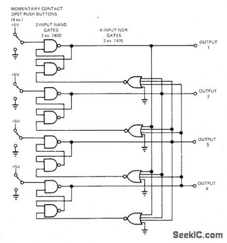
Arrangem ent provides low-cost equivalent of mechanically inteelocked switch assembly, while providing TTL compatibility and freedom from switch bounce. Momentary pressing of any pushbutton restores its associated RS flip-flop to normal and makes output of that channel high. Arrangement uses cross-coupled two-input NAND gates for each flip-flop, connected so each actuation produces an output and resets all other flip-flops. If two or more buttons are pushed simultaneously, all their channels will go high, but only last one released will stay on. Any number of channels may be added.—B.Brandstedt, Digital Interlocking Switch is Inex-pensive to Build, EDN Magazine, Dec. 15, 1972, p 42. (View)
View full Circuit Diagram | Comments | Reading(862)
1.8kHz Signal Generator Circuit
Published:2011/7/21 0:30:00 Author:Joyce | Keyword: 1.8kHz , Signal Generator
The circuit in the figure selects temperature coefficient for the best working state and reasonable distribution of the components of the resonance loop. Alternating current and stabilized voltage are used at both ends of the resonance so that excellent output amplitude and frequency stability is received. The working temperature is +25℃-±20℃. Even when the power supply voltage changes in the range of -40% at -24V, the frequency △ f will not be greater than 2Hz,and output level △ dB will not be more than 0.26 dB.
(View)
View full Circuit Diagram | Comments | Reading(635)
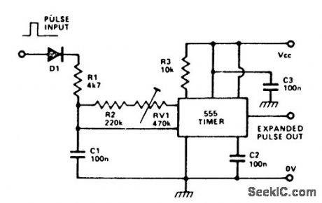
CARRIER_OPERATED_RELAY
Published:2009/6/29 4:00:00 Author:May
View full Circuit Diagram | Comments | Reading(6)
BOUNCELESS_MAKE_BREAK
Published:2009/6/29 4:00:00 Author:May
Circuit eliminates switch bounce problems during closing as well as opening. When switch is closed, Q output of flip-flop goes to logic 1 for delay period determined by RC time constant. Releasing switch operates NAND gate, making its output go to logic 1. This charges C through R until reset level is reached. Flip-flop then resets, changing Q output to logic 0. Values for R and C are chosen according to bounce duration of switch used. Fortypical 1-ASPST switch, 10,000 ohms and 0.41 μF were used.—L. F, Walsh and T. W. Hill, Make-and-Break Bounceless Switching, EDN|EEE Magazine, July 15, 1971, p 49. (View)
View full Circuit Diagram | Comments | Reading(791)
2100Hz Signal Generator Circuit
Published:2011/7/22 1:58:00 Author:Joyce | Keyword: 2100Hz, Signal, Generator Circuit
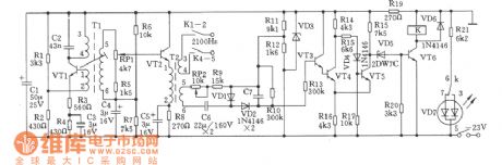
The circuit is as shown in the figure. The 2100 Hz signal generator is composed of oscillation, buffer amplifier and alarm circuit. VT1 and related components constitute the collector tuned oscillator. R1, R2 are bias resistances of VT1 .R3, R4 are emitter resistances which are used to stabilize dc working point. At the same time, R3 also provides negative feedback to improve the performance of the oscillator. C3 is the bypass capacitor of R4, which will reduce the wastage of signals. Coil L3-4 of transformerT1 and capacitance C2 constitute the 2100 Hz oscillation tank circuit. The positive feedback voltage is obtained from coil L1-2. (View)
View full Circuit Diagram | Comments | Reading(663)
Low Frequncy Signal Generator(2Hz、4Hz、60Hz、120Hz ect) Circuit
Published:2011/7/22 2:08:00 Author:Joyce | Keyword: Low Frequncy , Signal , Generator
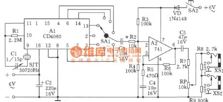
Low frequency signal generator can be used to measure the sensitivity, frequency response, frequency compensation and tone control of amplifier circuit. It also can be used to repair low frequency amplifiers. So it is a very useful measuring instrument. It also can be used as signal source of digital clock. According to the practical needs, the user can choose from 8 fixed frequencies output by the signal generator. The output amplitude is divided into two gears: 0 ~ 0.1 V, 0 ~ 1 V which can be adjusted continuously. Principle of the circuit is as shown in the figure. Integrated circuit CD4060 is a 14-level frequency divider installed with oscillator. (View)
View full Circuit Diagram | Comments | Reading(1299)
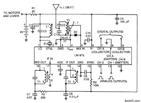
RADIO_CONTROL_MOTOR_SPEED_CONTROLLER
Published:2009/6/29 3:59:00 Author:May
View full Circuit Diagram | Comments | Reading(1037)
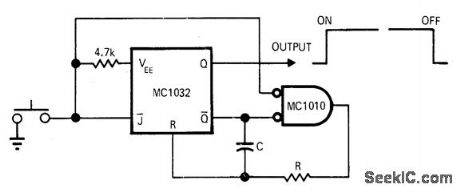
DEBOUNCING_WITH_COUNTER
Published:2009/6/29 3:59:00 Author:May
Circuit uses CMOS counteridecoder with any inexpensive 200-Hz or higher clock such as CMOS two-gate oscillator or 555 timer. Signal to be debounced is fed directly to reset input of counter, with no preconditioning. When contact is made by switch, counter unclears and starts counting up. Each bounce of contact resets counter, so it cycles between states 0 and 1 until contacts settle. Counter then delivers clean nonoverlapping pulses to remaining output lines, any of which may be used as conditioned output signal.When counter reaches state 7, it inhibits itself to prevent repeated pulsing of output lines. When switch is opened, cycling action is repeated during bounces, with output never going higher than state 1. After bouncing, counter is held in clear state ready for next closing.—L. T. Hauck, Solve Contact Bounce Problems Without a One-Shot, EDN Magazine, Sept, 5, 1975, p 80 and 82 (View)
View full Circuit Diagram | Comments | Reading(830)
TONE_ACTUATED_RELAY
Published:2009/6/29 3:57:00 Author:May

The circuit is built around the LM567 tone decoder IC that requires about 100 millivolts at its operating frequency. The frequency is set by a 10 K variable resistor and can be between 700 and 1500 Hz. When a tone at the set fre-quency is present, the 567's output goes low to energize a relay through a 2N3906 PNP transistor. (View)
View full Circuit Diagram | Comments | Reading(2518)
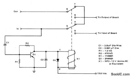
AUTOMATIC_TURN_OFF_FOR_TV_SET
Published:2009/6/29 3:51:00 Author:May
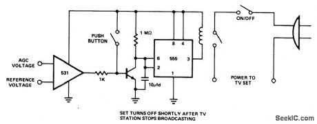
View full Circuit Diagram | Comments | Reading(742)
ROTARY_SWITCH_DEBOUNCE
Published:2009/6/29 3:50:00 Author:May
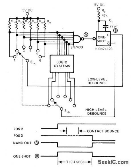
Outputs from mono (one-shot) provide common retums for rotary switch. Multi-input NAND gate, tied to normally high signals from one deck of rotary swhch, instantly detects opening of one contact and triggers mono. Mono then simulates open contact for interval determined by values used for R7 and C1; for values shown, delay is 400 ms.—E. S. Peltzman, Circuit Eliminates Rotary-Switch Bounce Problems, EDN Magazine, April 20, 1978, p 132. (View)
View full Circuit Diagram | Comments | Reading(1142)
| Pages:1246/2234 At 2012411242124312441245124612471248124912501251125212531254125512561257125812591260Under 20 |
Circuit Categories
power supply circuit
Amplifier Circuit
Basic Circuit
LED and Light Circuit
Sensor Circuit
Signal Processing
Electrical Equipment Circuit
Control Circuit
Remote Control Circuit
A/D-D/A Converter Circuit
Audio Circuit
Measuring and Test Circuit
Communication Circuit
Computer-Related Circuit
555 Circuit
Automotive Circuit
Repairing Circuit