
Circuit Diagram
Index 1249
Power_op_amp_follower_inverter
Published:2009/7/24 23:13:00 Author:Jessie
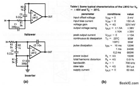
This circuit shows an LM12 power op amp connected as both a follower and an inverter, with input compensation to reduce bandwidth and increase stability. Figure 10-46B shows typical characteristics for the LM12, which is compensated for unity-gain feedback, and a small-signal bandwidth of 700 kHz. The LM12 is housed in a TO-3 package and requires a heatsink (because of the high power). Figure 10-46C shows the heatsink surface area required for temperature rise and power dissipation. National
(View)
View full Circuit Diagram | Comments | Reading(873)
SINGLE_ENDED_MICROPHONE_PREAMP
Published:2009/6/29 2:32:00 Author:May
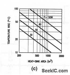
Noise performance is -69 dB below 2-mV input reference point. Use metal-film resistors for R2 and R5. Total harmonic distortion is less than 0.1%. Gain is set by ratio of R4 to R2 and is 52 dB.- Audio Handbook, National Semicon-ductor, Santa Clara, CA, 1977, p 2-37-2-40. (View)
View full Circuit Diagram | Comments | Reading(768)
Replacing_a_9_V_battery_with_two_AA_cells
Published:2009/7/24 23:12:00 Author:Jessie
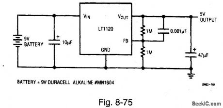

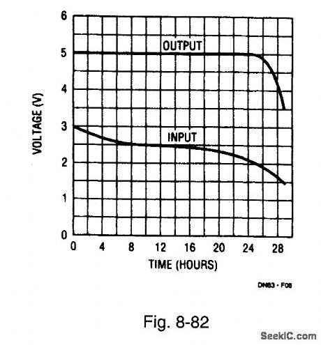
Figure 8-75 shows an LT1120 linear regulator used with a 9-V battery to provide a 5-V, 30-mA output. Figure 8-76 shows an LT1173-5 switching regulator used with a 9-V battery to provide the same output. Figure 8-77 shows the same LT1173-5 used with two AA cells to provide the same output (step-up). Figure 8-78 shows efficiency for the step-down circuits. Figure 8-79 shows efficiency for the step-up (two-AA cell) circuit. The battery life for the three circuits is shown in Figs. 8-80, 8-81, and 8-82, respectively. A study of these curves shows that efficiency remains higher, and battery life is longer, with the two AA cells, for the same voltage and current output. LINEAR TECHNOLOGY, DESIGN NOTE 63, P. 1, 2. (View)
View full Circuit Diagram | Comments | Reading(684)
VOLTAGE_WINDOW_COMPARATOR
Published:2009/6/29 2:32:00 Author:May
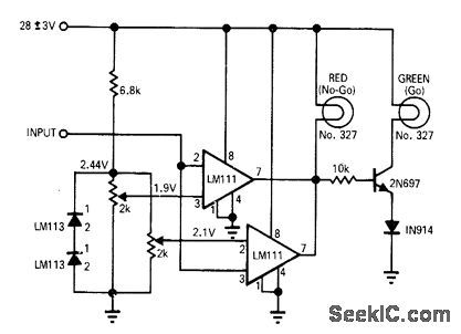
Use of LM111 opamps minimizes number of components required to turn on green indicator Iamp when input voltage is between predetermined limits set by 2K pots. Similar circuit using 741 opamps requires total of 31 components. Improved eircuit draws only 120 nA from voltage level being monitored, and operates within 0.3% threshold level stability using single unregulated supply varying ±3 V from 28 V.—D. Priebe, Comparators Compared, EDN|EEE Magazine, Oct. 1, 1971, p 61, (View)
View full Circuit Diagram | Comments | Reading(2713)
TIMING_CIRCUIT
Published:2009/6/29 2:31:00 Author:May
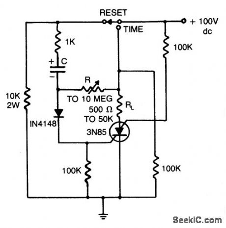
Load current starts approximately 0.5 RC after the switch IS thrown. (View)
View full Circuit Diagram | Comments | Reading(0)
Alkaline_battery_switching_regulator
Published:2009/7/24 23:08:00 Author:Jessie
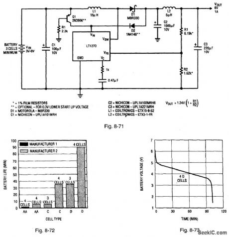
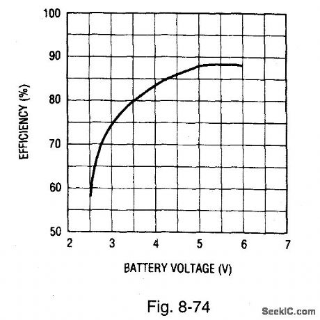

Figure 8-71 shows an LT1270 connected to provide a 6-V, 1-A output using three or four alkaline-battery cells (instead of NiCads). The output voltage can be changed by the selection of resistors R1 and R2, using the VOUT equation (as is the case with most switching regulators). Figure 8-72 shows alkaline-battery-life characteristics for a 6-W load. Figure 8-73 shows alkaline-battery-discharge characteristics for the same 6-W load. Figure 8-74 shows the efficiency for various alkaline-battery voltages. LINEAR TECHNOLOGY, DESIGN NOTE 41, P. 2. (View)
View full Circuit Diagram | Comments | Reading(1441)
POWER_OPAMPS_IN_BRIDGE
Published:2009/6/29 2:31:00 Author:May
Bridge configuration is theoretically capable of 4 times power output of conventional quasicomplementary or complementary-sym metry amplifier. Use of bridge circuit in automotive AMiFM stereo re-ceiver requires suitable protection of modules. Article covers incorporation of protective controls in single module with dual opamps.-E. R.Buehler and B. D. Schertz, Fault Protection of Monolithic Audio Power Amplifiers in Severe Environments, IEEE Transactions on Consumer Electronics, Aug. 1971, p 418-423. (View)
View full Circuit Diagram | Comments | Reading(681)
ON_OFF_CONTROLLER
Published:2009/6/29 2:31:00 Author:May
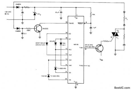
The ac line-operated on/off controller is a simple, reliable solid-state altemative to a mo-tive driven cam switch. Time 1 and time 2 are programmed by diodes to be 8 hours and 20 hours respectively. The TIM1 output is buffered by a transistor to supply gate current to a triac which switches the output load. When power is applied to the circuit, the output load is switched on for 8 hours then off for 20 hours repeatedly. (View)
View full Circuit Diagram | Comments | Reading(995)
Op_amp_instrumentation_amplifier_with_adjustable_gain
Published:2009/7/24 23:07:00 Author:Jessie
This circuit is similar to that of Fig. 10-35, except that the voltage gain can be adjusted (from 1 to 300) by selection of R6. With the values shown for R2/R4 and R3/R5, CMRR is 60 dB. (View)
View full Circuit Diagram | Comments | Reading(924)
Feedforuoard_compensation_to_speed_op_amp_response
Published:2009/7/24 23:05:00 Author:Jessie
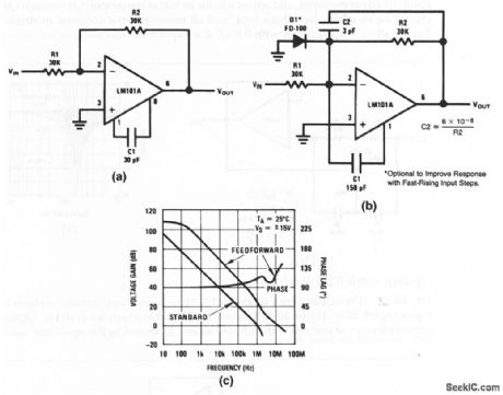


The slew rate and bandwidth of most op amps can be increased using feedforward compensation. Figure 10-44A shows an LM101A with standard compensation, while Fig. 10-44B shows feedforward compensation. Figure 10-44C shows a comparison of the two methods. Feedforward is accomplished by connecting C1 between the inverting input and one of the compensation pins (to eliminate internal pnps from the signal path at high frequencies). Unity gain bandwidth is extended from about 1 to 10 MHz, while the slew rate is increased from about 0.5 to 10 V/μS. (View)
View full Circuit Diagram | Comments | Reading(872)
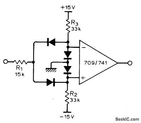
DUAL_LIMITS
Published:2009/6/29 2:30:00 Author:May
View full Circuit Diagram | Comments | Reading(641)
SIMPLE_FIELD_STRENGTH_METER
Published:2009/6/29 2:29:00 Author:May
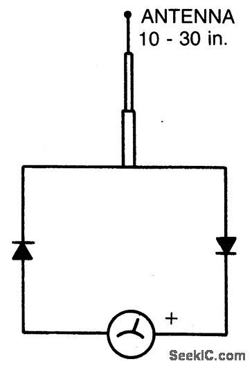


Circuit Notes
The circuit is frequency selective. It has been used from 2 meters through 160 meters. The telescoping antenna may be adjusted to its shortest length when working at 2 meters to keep the needle on the scale. Meter should be a 100 microamp to a 500 microamp movement. The diodes are germanium type, such as 1N34, etc. Silicon diodes will also work, but they are a bit less sensitive. (View)
View full Circuit Diagram | Comments | Reading(1968)
Dual_35_V_to_5_V_12_V_supply
Published:2009/7/24 23:04:00 Author:Jessie
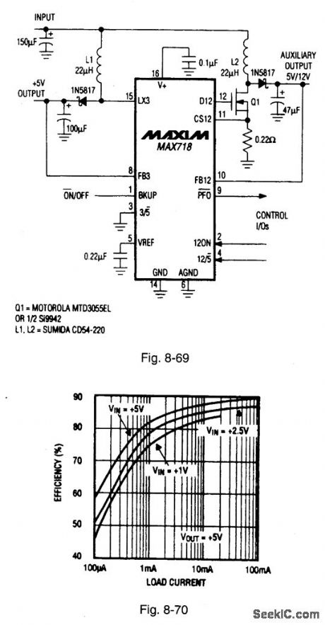
Figure 8-69 shows a MAX718 controller connected to provide 5 V and 12 V from a 3.3-V supply. Figure 8-70 shows the efficiency curves. This circuit is designed for those applications that require a 3.3-V to 5-V converter to supply power for peripheral equipment, and a +12-V supply for flash-memory programming. The circuit delivers 5 V at 400 mA, and 12 V at 120 mA when powered from a 3.3-V (±10%) supply. The 12-V output can be programmed to 5 V, under logic control without external switches or pullup. The input voltage is 0.9 V to VOUT with 1.4-V no-load start-up. Quiescent current is 140 μA for 5 V, and 500 μA for both 5 V and 12 V. The switching frequency is 0.5 MHz. MAXIM BATTERY MANAGEMENT CIRCUIT COLLECTION, 1994, P. 42. (View)
View full Circuit Diagram | Comments | Reading(682)
ELECTRONIC_EGG_TIMER
Published:2009/6/29 2:29:00 Author:May
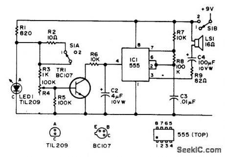
The IC functions as an af multivibrator which is controlled by the external transistor. S1A/B is the on-off toggle switch. (View)
View full Circuit Diagram | Comments | Reading(1084)
Op_amp_notch_filter_adjustable_Q
Published:2009/7/24 23:03:00 Author:Jessie


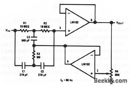
This circuit uses two LM102s to form a 60-Hz notch filter with adjustable Q. The response should fall within the shaded area of Fig. 10-42B. Remember that R4 sets the Q, not the notch frequency. Other frequencies can be selected using the equations of Fig. 10-42. (View)
View full Circuit Diagram | Comments | Reading(967)
SCR automatic delay light switch circuit diagram
Published:2011/8/1 1:54:00 Author:Ecco | Keyword: SCR , automatic delay , light switch
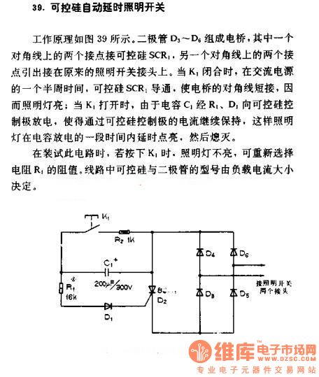
SCR automatic delay light switch
Working principle is shown in Figure 39. The diode D1 ~ D6 make up bridge, the two contacts on one of the diagonalis connected to SCR1, andthe other two contacts on the diagonal leads are connecting to the original light switch. When K1 is closed, in a half week time of AC power, SCR1 turns on, so that the diagonal of the bridge short connected, so lights are bright; when K1 is open, the capacitor C1 discharges through R1, D1 to the SCR system-level, making the current of SCR system-level maintain. So light is turned on in the capacitor discharging delayedtime, then turned off.
When peopleinstall this circuit, if pressing K1, lights off, you can re-select the resistance of resistor R1. The model of SCR and diode circuit determined by the size of the load current. (View)
View full Circuit Diagram | Comments | Reading(1482)
Op_amp_notch_filter_high_Q
Published:2009/7/24 23:02:00 Author:Jessie
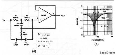
This circuit uses a single LM102 in the twin-T configuration to form a high-Q notch filter. Figure 10-42B shows the filter characteristics at 60 Hz. Other frequencies can be selected with different values, as shown by the equations. (View)
View full Circuit Diagram | Comments | Reading(1380)
PRECISION_SOLID_STATE_TIME_DELAY_CIRCUIT
Published:2009/6/29 2:28:00 Author:May
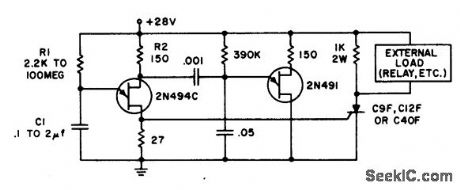
Time delays from 0.3 milliseconds to over three minutes are possible with this circuit without using a tantalum or electrolytic capacitor. The timing interval is initiated by applying power to the circuit. At the end of the timing interval, which is determined by the value of R1C1, the 2N494C fires the controlled rectifier. This places the supply voltage minus about one volt across the load. Load currents are limited only by the rating of the controlled rectifier which is from 1 ampere up to 25 am-peres for the types specified in the circuit. A calibrated potentiometer could be used in place of R1 to permit setting a predetermined time delay after one initial calibration. (View)
View full Circuit Diagram | Comments | Reading(858)
Low_power_33_V_to_5_V_supply
Published:2009/7/24 23:01:00 Author:Jessie
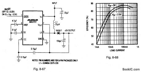
Figure 8-67 shows a MAX731 connected to provide 5 V from a 3.3-V supply. Figure 8-68 shows the efficiency curves. This PWM boost regulator is designed for low-noise, battery-powered applications, such as cellular phones or sub-notebook computers without rotating disk drives (where the maximum +5-V load is 2 W or less). The input voltage range is 1.4 V to 5 V, with a quiescent current of 2 mA, and a maximum load current of 350 mA. The no-load start-up voltage is 1.8 V. The switching frequency is 170 kHz, and the shutdown current is 35 pt,A. MAXIM BATTERY MANAGEMENT CIRCUIT COLLECTION, 1994, P. 41. (View)
View full Circuit Diagram | Comments | Reading(647)
True_rms_detector
Published:2009/7/24 23:00:00 Author:Jessie
This circuit provides a dc output equal to the rms value of the input. Accuracy is typically 2% for a 20-V pp input from 50 Hz to 100 kHz. To calibrate, apply 10 Vdc at the input, and adjust R10 for 10V dc at the output.Q1 through Q4 should be matched, have high beta, and all mounted on a common heatsink. Bypass all Op amp supplies with 0.1-μF disc capacitors. (View)
View full Circuit Diagram | Comments | Reading(3667)
| Pages:1249/2234 At 2012411242124312441245124612471248124912501251125212531254125512561257125812591260Under 20 |
Circuit Categories
power supply circuit
Amplifier Circuit
Basic Circuit
LED and Light Circuit
Sensor Circuit
Signal Processing
Electrical Equipment Circuit
Control Circuit
Remote Control Circuit
A/D-D/A Converter Circuit
Audio Circuit
Measuring and Test Circuit
Communication Circuit
Computer-Related Circuit
555 Circuit
Automotive Circuit
Repairing Circuit