
Circuit Diagram
Index 1251
CLASS_B_WITHOUT_TAKEOVER_DISTORTION
Published:2009/6/29 2:25:00 Author:May
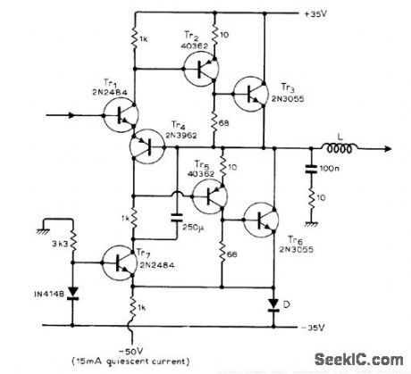
Circuit uses two transistor triplets in output stage, with quiescent current set at 15 mA by Tr7 which serves as constant-current source. For small signals, Tr1 and Tr4 can be regarded as long-tailed pair without tail. For positive signals, Tr1-Tr4 become active and behave as super emitter-follower, while Tr1 with Tr4-Tr6 serve for negative signals. One advantage of circuit is low output impedance.-N. M. Visch, A Novel Glass B Output, Wireless World, April 1975, p 166. (View)
View full Circuit Diagram | Comments | Reading(961)
WINDOW_DETECTOR
Published:2009/6/29 2:25:00 Author:May
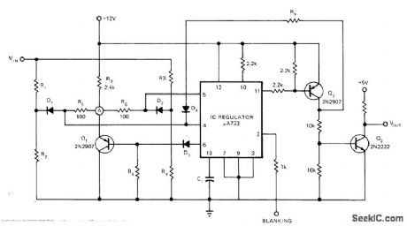


Uses one IC regulator to compare output voltages of two separate voltage dividers with fixed reference voltage. Resulting absolute error signal is amplified and converted to TTL-compatible Iogic signal. Voltage divider for lower limit of window detector is R1-R2 and for upper limit is R3-R4. Article covers circuit operation in detail.—N. Pritchard, Window Detector Uses 0ne IC Regulator, EDN Magazine, May 20, 1973, p 81 and 83. (View)
View full Circuit Diagram | Comments | Reading(0)
Precision_instrumentation_amplifier
Published:2009/7/24 23:25:00 Author:Jessie
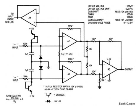
This circuit provides differential-input to single-ended-output conversion with accurate circuit gain. Amplifier characteristics are shown in the table. (View)
View full Circuit Diagram | Comments | Reading(0)
01_TO_90_SECOND_TIMER
Published:2009/6/29 2:25:00 Author:May
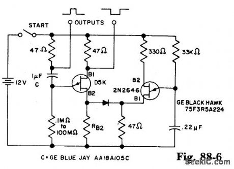
The timer interval starts when power is applied to circuit and terminates when voltage is applied to load. 2N2646 is used in oscillator which pulses base 2 of D5K. This reduces the effective L of D5K and allows a much larger timing resistor and smaller timing capacitor to be used than would otherwise be possible. (View)
View full Circuit Diagram | Comments | Reading(867)
5_V_from_two_to_thre_cells_with_low_noise
Published:2009/7/24 23:24:00 Author:Jessie
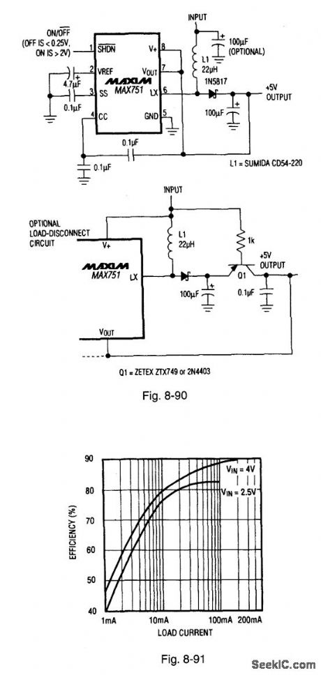
Figure 8-90 shows a MAX751 connected to provide a 5-V output. with a 2-V to 5-V input range, but with low nolse. This circuit provides a fixed-frequency PWMalternative to the pulse-skipping control scheme usually found in low-voltageswitching-regulator ICs. (The noise generated by switching regulators is a major problem in many portable products such as cellular phones and medicalinstruments,) The trade-offs for low-noise operation are increased quiescent supply current and lower efficiency for light loads.The quiescent current with a VIN of 3 V is 1.2 mA, with a maximum load current of 100 mA (with VIN=2.7 V). The circuit has a shutdown current of 30 μA and a fixed oscillator frequency of 170kHz,The no-load start-up is 1.2 V. Figure 8-91 shows the efficiency curves. MAXIMBATTERY MANAGEMENT CIRCUIT COLLECTION 1994 P. 13. (View)
View full Circuit Diagram | Comments | Reading(628)
COMPARATOR_DRIVES_LED
Published:2009/6/29 2:24:00 Author:May
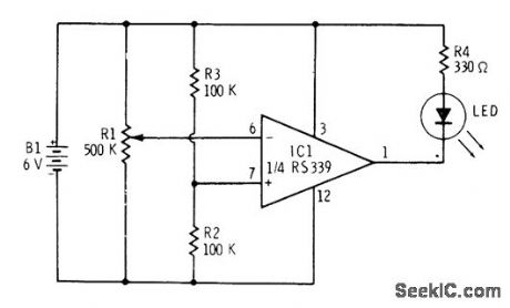
Simple classroom demonstrator of comparator action uses one section of RS339 quad comparator. Reference voltage applied to positive input of comparator is half of supply voltage. R1 serves as voltage divider applying variable voltage to inverting input. When voltage applied to pin 6 by R1 exceeds reference voltage on pin 1, comparator switches on and LED lights. R4 is chosen for use with Radio Shack 276-041 red LED.—F.M.Mims, Integrated Circuit Projects, Vol. 6, Radio Shack, Fort Worth TX, 1977, p 33-41. (View)
View full Circuit Diagram | Comments | Reading(956)
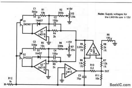
Power_op_amp_master_slave
Published:2009/7/24 23:24:00 Author:Jessie
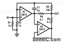
This circuit shows two LM12s (Fig. 10-46) connected in a master/slave configuration to increase the load current capability. Notice that a separate control amplifier (such as used in Fig. 10-47) is not required. However, the high-frequency performance of the master/slave configuration is not as good as with the Fig. 10-47 circuit. (View)
View full Circuit Diagram | Comments | Reading(725)
TIME_DELAYED_RELAY_FOR_PATIO_LIGHT,GARAGE_LIGHT,ENLARGER_PHOTOTIMER,ETC
Published:2009/6/29 2:24:00 Author:May
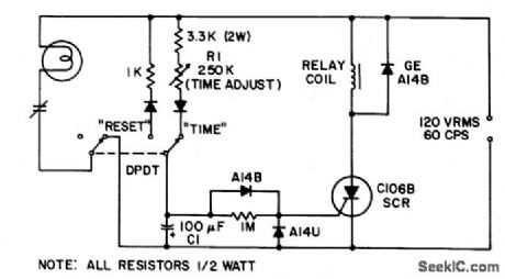
This simple timing circuit cat: delay an output switching function from.01 seconds to about 1 minute. The SCR is triggered by only a few microamps from the timing network R1-C1 to energize the output relay. (View)
View full Circuit Diagram | Comments | Reading(704)
Electronic hypnotic device 1
Published:2011/8/1 2:50:00 Author:Ecco | Keyword: Electronic , hypnotic device
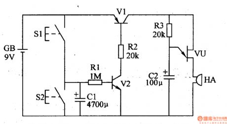
This example describes the electronic hypnotic device made by discrete electronic components , which will issue the simulated dripping water sound of tick, tick, tick when working. If insomnia intently listens to this sound of water, then he will quickly fall asleep. The working principle.The electronic circuit is composed of the oscillator circuit and timer circuit, and it is shown as Figure 9-138.
Oscillator is a relaxation oscillator composed of single-junction transistor VU and resistors R2, capacitor C2 , which outputs the narrow pulse signal with width in 1.2ms, interval in 1.4s, it emits the dropping sound by HA. Timer circuit consists of transistors Vl, V2, and starting button Sl, termination button S2 etc. It is used to control the oscillator work. Pressing the Sl, capacitor Cl is fully charged at the moment, V2 is on as the base being positively biased, so that Vl is also conducting, +9 V voltage is added to the oscillator Vl (c, e pole), the oscillator makes oscillation. About lh, Cl end the discharging (via resistor Rl, and V2, b, e node discharge), V2 and V1 are off, the oscillator stops. In the oscillator working period, If you click S2, then the Cl will discharge rapidly through the S2, so that V2, V1 are closing, the oscillator stops. (View)
View full Circuit Diagram | Comments | Reading(1069)
555 automobile device circuit diagram
Published:2011/7/22 1:22:00 Author:Sophia | Keyword: automobile device circuit
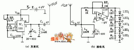
As shown, the car recording device includes the transmitter and receiver. Transmitter constitute oscillator of midband frequency with the core 555, oscillator frequency should be slightly lower than carrier frequency 535KHZ of the AM broadcast, the frequency value depends on R1, RP1, C1, namely f = 1.44 / (RP1 +2 R1). C1, L1, C2 constitute the output resonant circuit, which selects frequency, and then transmit through the C3 by the antenna. Receiving circuit is composed of the input frequency-selective network and 741 op amp. Amplification factor of amplifier depends on RP2/R2. LED1 ~ LED5 is used to indicate received signal strength. Along with the strengthening of the signal, luminotron will be lighted up by the order! !
(View)
View full Circuit Diagram | Comments | Reading(1134)
Linear_FM_detector
Published:2009/7/24 23:43:00 Author:Jessie
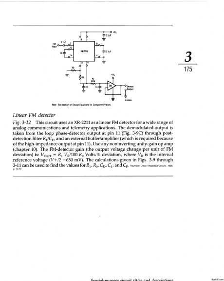
This circuit uses an XR-2211 as a linear FM detector for a wide range of analog communications and telemetry applications. The demodulated output is taken from the loop phase-detector output at pin 11 (Fig. 3-9C) through post-detection filter RF/CF, and an external buffer/amplifier (which is required because of the high-impedance output at pin 11). Use any noninverting unity-gain op amp (chapter 10). The FM-detector gain (the output voltage change per unit of FM deviation) is: VOUT=R1 VR/100 R0 Volts/% deviation, where VR is the internal reference voltage (V+/2 -650 mV). The calculations given in Figs. 3-9 through 3-11 can be used to find the values for R1, R0, CD, C1, and CF. (View)
View full Circuit Diagram | Comments | Reading(2202)
Motor vehicle steering flasher 13
Published:2011/8/1 2:49:00 Author:Ecco | Keyword: Motor vehicle , steering flasher
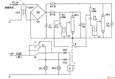
The motor vehicle steering flasher described in the example can automatically turn the flash frequently when installing on the motorcycle, it can remind the traveling vehicles to improve road safety.
The motorcycle steering circuit is composed of the power circuit, the first strobe circuit, strobe circuit and control circuit; it is shown as Figure 7-22.
Power circuitis composed ofthe fuse FU, step-up transformer Tl, rectifier bridge UR and filter capacitor Cl.
The first strobe circuit consists of resistors Rl, R2, capacitor C2, C3, and the flash tubeHL3 and trigger transformer T2.
Control circuitconsists ofthe manual switch Sl, motorcycle turn signal switch S2, the relay K and diode VDl, VD2 and so on.
Rl and R4 select thelW metal film resistors or wire wound resistors; R2 and R3 select 1/2W carbon film resistor.
Cl and C3, C5 select the electrolytic capacitors with voltagebeing 400V or more; C2 uses the polyester capacitor with the voltagein 630V or CBB capacitor.
VDl and VD2 use 1N4001 or lN4007 silicon rectifier diodes.
UR selects IA, 600V rectifier bridge reactor.
Tl uses 5W, l2/220V power transformer; m and T3 are all made of flash-specific trigger transformer.
S1 selects double-toggle switch.
HL3 and HL4 select flash tube for camera. (View)
View full Circuit Diagram | Comments | Reading(802)
Basic_power_op_amp_voltage_regulator
Published:2009/7/24 23:41:00 Author:Jessie
This circuit shows an LM12 (Fig.10-46) connected as a basic positive regulator with 0- to 70-V output range (set by R2). The output will source or sink current. Current drawn is less than 150 mA, except when sinking load current. (View)
View full Circuit Diagram | Comments | Reading(786)
5_V_from_four_cells_switchabie_step_up_step_down
Published:2009/7/24 23:41:00 Author:Jessie
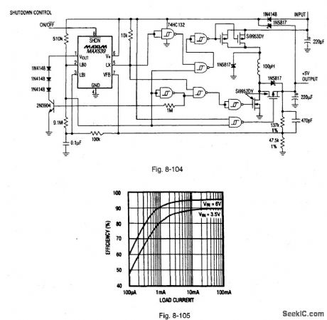
Figure 8-104 shows a MAX639 connected to provide a 5-V output from four cells,This circuit switches from step-down to step-up mode as the battery output fallsbelow 5 V The circuit operates over an input-voltage range of 3 V to 6.5 V. with aquiescent current (VIN=5.5 V) of 50 μA, and 110 μA for a VIN of 4.5 V The maximum load current is 200 mA with a VIN of 3.75 V Battery life is 17.2 hours(using four alkaline AA cells with 100-mA load).Figure 8-105 shows the efficiencycurves.MAXIM BATTERY MANAGEMENT CIRCUIT COLLECTION, 1994. P. 24.
(View)
View full Circuit Diagram | Comments | Reading(651)
Tone_detection
Published:2009/7/24 23:40:00 Author:Jessie

This circuit is similar to that of Fig. 3-9, but shows the XR-2211 (Fig.3-9C) connected as a tone detector. Q and Q are normally high and low, respectively. When a tone is present within the PLL detection band, Q and Q reverse states (for the duration of the tone). Each output (pins 5 and 6) can sink 5 mA of load current. RL1/RL2 pull-down resistors are required since both outputs are open-collector. The circuit can be optimized for any tone-detection application by the choice of R0, R0, C0, C1, and CD. For a given input-tone frequency, fs, these parameters are calculated as follows:Choose R0 in the range of 15 to 100 kΩ (arbitrary).Calculate C0 to set center frequency, f0 /fs using= C0= l/R0/fs.Calculate R1 to set bandwidth using: R1=R0(f0/▲f). Notice that the total detection bandwidth covers the frequency range of f0±▲f.Calculate C1 for a given loop-damping factor using: C1= 0.25 C0. Increasing C1 improves the out-of-band signal rejection, but increase the PLL capture time.Calculate the minimum value of filter capacitance CD using: CD (in μF) 16/capture range in Hz. Large values of CD slow response time and small CD values can result in chatter.The following values are for a tone detector with a detection band of 1 kHz ±20 Hz. R0 is an arbitrary 20 kΩ (18 kΩ 5-kΩ pot). C0=, 0.05 μF,R1=1 MΩ, C1= 0.013 μF, CD = 0.42 μF (a capture range of 38 Hz instead of 40 Hz). Fine tune the center frequency with Rx. (View)
View full Circuit Diagram | Comments | Reading(3125)
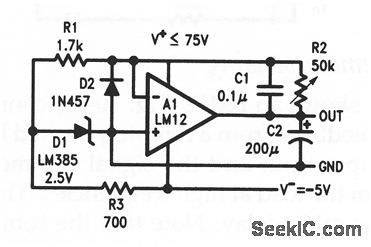
Power_op_amp_with_current_limiting
Published:2009/7/24 23:40:00 Author:Jessie
The positive and negative limiting currents of the LM12 (Fig. 10-46) can be set precisely and independently down to 0 with R3 and R7. Alternately, the limits can be set programmed from a voltage supplied to R2 and R6. The LM12 is connected as an inverting amplifier with the output sensed across R10. This sense-voltage level is shifted to ground by A3, a differential amplifier that is made insensitive to the LM12 output level by trimming R9. (View)
View full Circuit Diagram | Comments | Reading(920)
The motor vehicle headlight auto-dimming controller 5
Published:2011/8/1 2:49:00 Author:Ecco | Keyword: motor vehicle, headlight, auto-dimming , controller
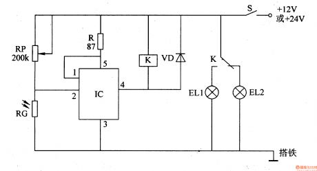
The motor vehicle headlight auto-dimming controller described in the example can automatically change the high beam into low beam at night, it improves the safety of driving at night.The working principle.The vehicle headlight auto-dimming controller circuit consists of photoresistor RG, electronic switch IC, potentiometer Rp, resistor R, the relay K, diode VD and other components, the circuit is shown as the figure 7-5.
Turning on the headlamp control switch S, RG is in a high impedance state due to no light exposure, the pin 2 of IC is in high potential, their internal electronic switch is off, pin 4 outputs high potential, K is in free state, the normally open contact is open, normally closed contact is connected, high beam EL2 is lit.
R chooses 1/2W metal film resistor or carbon film resistors.
RP selects small organic solid potentiometer.
RG uses a photosensitive resistor with light resistancebeing less than or equal to lOkΩ, dark resistancebeing greater than 5OOkΩ.
VD uses lN4007 silicon rectifier diode.
IC selects TWH8751 high-power electronic switching circuit.
K selects a l2V or 24V (supply voltage is according to motor vehicle) small DC relay.
(View)
View full Circuit Diagram | Comments | Reading(1891)
5_V_from_four_cells_inverter_or_flyback
Published:2009/7/24 23:39:00 Author:Jessie
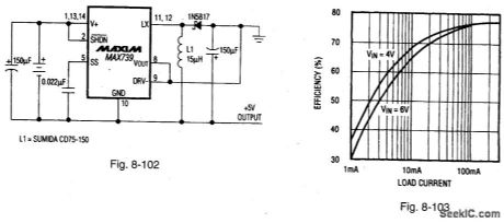
Figure 8-102 shows a MAX739 connected to provide a 5-V output from four cells.This circuit uses the MAX739 as an inverter with a battery-referenced output.Theinput voltage range IS 3.8 V to 11 V with a no-load startup of 4 V maximum. Quiescent current (VIN=5 V)IS 1.8 mA with a maximum load current of 200 mA.Shutdown current is 1 μA, and battery life is 13.5 hours (using four alkaline AAcells, vith a 100-mA load). Figure 8-103 shows the efficiency curves. MAXIM BATTERY MANAGEMENT CIRCUIT COLLECTION, 1994 P.23.
(View)
View full Circuit Diagram | Comments | Reading(671)
5_V_from_four_cells_preregulation
Published:2009/7/24 23:37:00 Author:Jessie
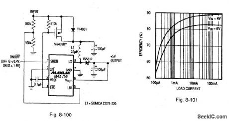
Figure 8-100 shows a MAX756 connected to provide a 5-V output from four cells. This circuit uses a diode and a PFET (in parallel) as a pre-regulator for the MAX756 boost regulator. The input voltage range is 2 V to 6.2 V, with a no-load start-up of 1.5 V, The quiescent current (VIN = 5 V) is 70 μA, with a maximum load current of 400 mA. The shutdown current is 55 μA, and battery life is 15.5 hours (using four alkaline AA cells with a 100-mA load). Figure 8-101 shows the efficiency curves, MAXIM BATTERY MANAGEMENT CIRCUIT COLLECTION, 1994, P. 22. (View)
View full Circuit Diagram | Comments | Reading(825)
3_V_33_V_from_three_cells_with_linear_regulation
Published:2009/7/24 23:28:00 Author:Jessie
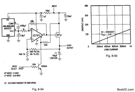
Figure 8-94 shows a MAX872 voltage reference and an ICL7611 micropower op amp connected to form a linear regulator for a 3-V/3.3-V supply. This circuit is particularly effective with NiCad and NiMH batteries. The end of life for such cells is about 1 V, so a linear regulator (with very low dropout) can be used in place of a switching regulator or charge pump. The dropout characteristics for the circuit are shown in Fig. 8-95, and depend primarily on the characteristics of Q1. When the circuit is used with low voltage, such as a three-cell battery, Q1 must have a gate-threshold voltage below that of the lowest battery voltage. For example, the RDS(ON) for the Si9433 is guaranteed at a VGS of 2.7 V. The circuit will operate at input voltages from 3 V to 15 V. The quiescent current (VIN = 6.5 V) is 40 μA when the circuit is operated in the low-power mode, but it increases to 70 μA in the high-power mode. The maximum load current is 1 A in high-power and 5 mA in low-power. The high - and low-power modes are selected by logic at the MODE SELECT input. High-power mode is selected when the input is high. MAXIM BATTERY MANAGEMENT CIRCUIT COLLECTION, 1994, P. 15. (View)
View full Circuit Diagram | Comments | Reading(1379)
| Pages:1251/2234 At 2012411242124312441245124612471248124912501251125212531254125512561257125812591260Under 20 |
Circuit Categories
power supply circuit
Amplifier Circuit
Basic Circuit
LED and Light Circuit
Sensor Circuit
Signal Processing
Electrical Equipment Circuit
Control Circuit
Remote Control Circuit
A/D-D/A Converter Circuit
Audio Circuit
Measuring and Test Circuit
Communication Circuit
Computer-Related Circuit
555 Circuit
Automotive Circuit
Repairing Circuit