
Circuit Diagram
Index 1242
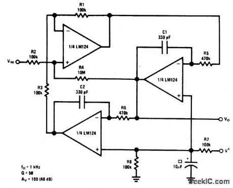
BIQUAD_RC_ACTIVE_BANDPASS_FILTER
Published:2009/6/29 21:30:00 Author:May
View full Circuit Diagram | Comments | Reading(843)
Voltage_follower_with_capacitive_load_above_100_pF
Published:2009/7/24 21:58:00 Author:Jessie
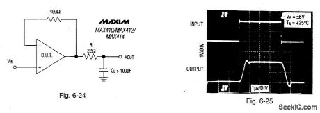
Figure 6-24 shows a voltage-follower circuit with a capacitive load above 100 pF.Figure 6-25 shows the waveforms. (see Fig. 6-1 for pin configurations). Resistor R1 isolates the load capacitance from the amplifier output to prevent oscillation.MAXIM NEW RELEASES DATA BOOK, 1994, P. 3-41. (View)
View full Circuit Diagram | Comments | Reading(740)
Voltage_follower_with_capacitive_load_100_pF
Published:2009/7/24 21:58:00 Author:Jessie
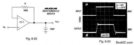
Figure 6-22 shows a basic voltage-follower circuit with a capacitive load. Figure 6-23 shows the waveforms (see Fig. 6-1 for pin configurations). This circuit is suitable for capacitive loads up to about 100 pF. MAXIM NEW RELEASES DATA BOOK, 1994 P. 3-41. (View)
View full Circuit Diagram | Comments | Reading(754)
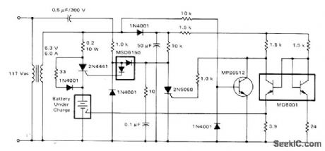
12_V_AUTOMATIC
Published:2009/6/29 21:29:00 Author:May
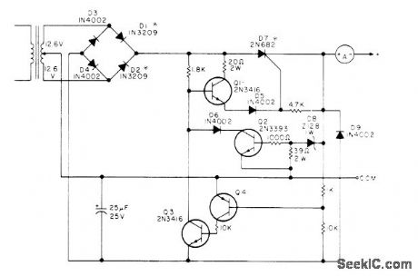
Circuit of Heathkit GP-21 automatic charger is self-controlling (Q1 and Q2) and provides protection against shorted or reversed battery leads (Q3 and Q4). Zener D8 is not standard value, so may be obtainable only in Heathkits. D1, D2, and D7 should all be on one heatsink.-H. Olson, Battery Chargers Exposed, 73 Magazine, Nov. 1976, p 98-100 and 102-104. (View)
View full Circuit Diagram | Comments | Reading(2891)
Negative_reference__25_V
Published:2009/7/24 21:57:00 Author:Jessie
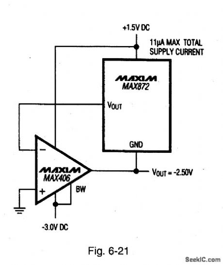
Figure 6-21 shows a MAX406 combined with a low-dropout MAX872 to form a precise -2.5-V reference that requires no external components. Typically, the MAX872 requires two external resistors. Maximum current drain is 11 μA. There is no degradation of voltage because of load regulation and no compensation is needed for load capacitance. The supplies need not have precise regulation. The positive supply can be as low as 1.1 V with the negative supply as low as 2.7 V. MAXIM NEW RELEASES DATA BOOK, 1994, P. 3-31. (View)
View full Circuit Diagram | Comments | Reading(619)
MULTIPLE_FEEDBACK_BANDPASS_FILTER
Published:2009/6/29 21:28:00 Author:May
View full Circuit Diagram | Comments | Reading(0)
A.C. Time Switch Controller Circuit
Published:2011/7/21 2:02:00 Author:Joyce | Keyword: A.C., Time Switch , Controller
As shown in the figure, the controller includes a depressurization and rectification relay, a monostable timing relay and an ac solid-state relay. The monostable time circuit is composed of 555, R2, RP1, and C4. Press AN, feet 3 of 555 will display a high level to dredge the ac output end of the ac solid-state relay and connect the load, at this time the timing will start .The timing time, namely the stable time of monostability is: td = 1.1 RP1C4.The longest timing time according to the parameters in the figure is about 30 minutes, which can be regulated by adjusting RP1.
(View)
View full Circuit Diagram | Comments | Reading(647)
BANDPASS_ACTIVE_FILTER_WITH_60_dB_GAIN
Published:2009/6/29 21:27:00 Author:May
View full Circuit Diagram | Comments | Reading(854)
Zero Volt Switch Circuit
Published:2011/7/21 21:21:00 Author:Joyce | Keyword: zero volt , switch
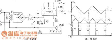
As shown in the figure, the zero volt switch circuit will produce trigger impulse when ac voltage passes zero. In order to achieve it, 555 is connected in the form of a comparator, and corresponding static offset voltage 0.7 ~ 1 V is set on the controlling end feet 5 .A LED is used as comparing device , as well as indication of the existence of the reference voltage . The oscillogram of working process is as shown in figure (b). Here, to illustrate the problem, sine wave is drawn as triangle wave, but analysis of the process will not be influenced.
(View)
View full Circuit Diagram | Comments | Reading(741)
Remotely_powered_sensor_amplifier
Published:2009/7/24 21:56:00 Author:Jessie
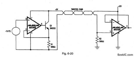
Figure 6-20 shows a simple two-wire current transmitter that uses no power at the transmitting end, except from the transmitted signal itself. At the transmitter, a 0-V to 1-V input drives both a MAX406 and an NPN transistor connected as a voltage-controlled current sink. The 0-mA to 2-mA output is sent through a twisted pair to the receiver and it develops a voltage across receiver sense resistor R2. The resulting sense voltage is buffered by another MAX406, producing a 0-V to 1-V ground-referenced output signal. R1 and R2 should be well matched. The MAX406 supply current is added to the 0-mA to 2-mA signal, resulting in a 500-μV offset at the output. This offset, in addition to the MAX406 input offset, varies with temperature. MAXIM NEW RELEASES DATA BOOK, 1994, P. 3-29. (View)
View full Circuit Diagram | Comments | Reading(0)
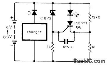
LED_INDICATES_LOW_VOLTAGE
Published:2009/6/29 21:27:00 Author:May
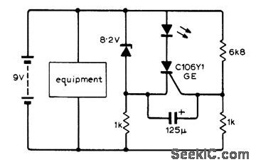
LED lights when output of 9-V rechargeable battery drops below minimum acceptable value of 8.3 V, to indicate need for recharging. Can also be used with transistor radio battery to indicate need for replacement. Zener is BZY85 C8V2 rated at 400 mW, with avalanche point at 7.7 V because of low current drawn by circuit. LED can be Hew-lett-Packard 5082-4440,-P.C. Parsonage, Low-Battery Voltage Indicator, Wireless World, Jan. 1973, p 31. (View)
View full Circuit Diagram | Comments | Reading(849)
Language Analysing Polygraph Circuit
Published:2011/7/20 3:52:00 Author:Joyce | Keyword: Language, Analysing, Polygraph
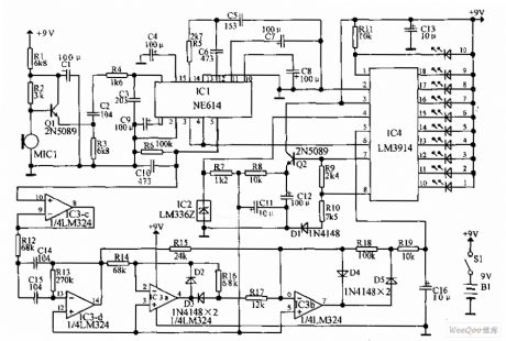
The signal of M1C1 is coupled to NE *, and signal RSSI output by feet 5 of logarithmic amplifiers IC1, IC1 is buffered by IC3-C of the op-amp LM324 to drive IC3-d, IC3-a, IC3-b to compose a detector for all wave crests. When output of IC3 = b is positive, the signal is integrated by R19 and C16. When language is stopped or the speaker is under great pressure, voltage of C16 will discharges through R18 and R19, for the time constant of C16 and R18, R19 is larger. It can make the bar chart DISP1 display signals which are increasing rapidly. During the suspension of language processing, a slow discharge will keep the value at display.
(View)
View full Circuit Diagram | Comments | Reading(1834)
1_kHz_BANDPASS_ACTIVE_FILTER
Published:2009/6/29 21:25:00 Author:May
View full Circuit Diagram | Comments | Reading(668)
NICAD_CHARGER
Published:2009/6/29 21:21:00 Author:May
Switch gives choice of two constant-current charge rates. With 10 ohmsfor R1, rate is 60 mA, while 200 ohms for R2 gives 3 mA. Silicon diodes CR1 and CR2 have combined voltage drop of 1.2 V and emitter-base junction of Q1 has 0.6-V drop, for net drop of 0.6 V across R1 or R2. Dividing 0.6 by desired charge rate in amperes gives resistance value.-M. Alterman, A Constant-Current Charger for Nicad Batteries, QST, March 1977, p 49. (View)
View full Circuit Diagram | Comments | Reading(1102)
Four_channel_sample_and_holdS_H
Published:2009/7/24 21:55:00 Author:Jessie
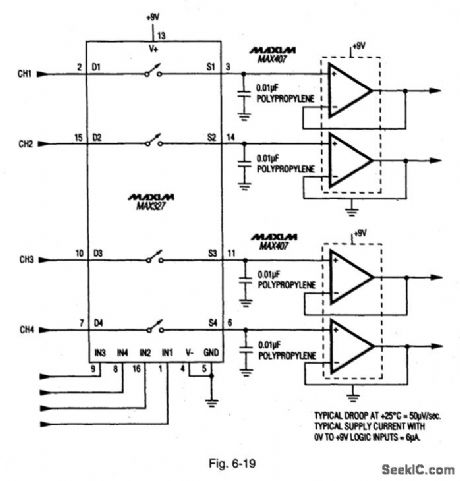
Figure 6-19 shows two MAX407s combined with a MAX327 to form a four-channel S/H circuit. See Fig. 6-18 for MAX407 pin configurations. MAXIM NEW RELEASESDATA BOOk, 1993, P. 3-30. (View)
View full Circuit Diagram | Comments | Reading(705)
LED_VOLTAGE_INDICATOR
Published:2009/6/29 21:13:00 Author:May
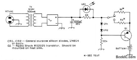
Circuit shown uses LED to indicate, by lighting up, that battery has been charged to desired level of 9 V. Circuit can be modified for other charging voltages. Silicon switching transistor can be used in place of more costlythyristor.-P. R. Chetty, Low Bat-tery Voltage Indication, Wireless World, April 1975, p 175. (View)
View full Circuit Diagram | Comments | Reading(1054)
THIRD_ELECTRODE_SENSES_FULL_CHARGE
Published:2009/6/29 21:13:00 Author:May
Circuit is suitable only for special nickel-cadmium batteries in which third electrode has been incorporated for use as end-of-charge indicator. Voltage change atthird electrode is sufficient to provide reliable shutoff signal for charger under all conditions of temperature and cell variations.-D. A. Zinder, Fast Charging Systems for Ni-Cd Batteries, Motorola, Phoenix, AZ, 1974, AN-447, p 7. (View)
View full Circuit Diagram | Comments | Reading(1189)
Buffered_pH_probe
Published:2009/7/24 21:53:00 Author:Jessie
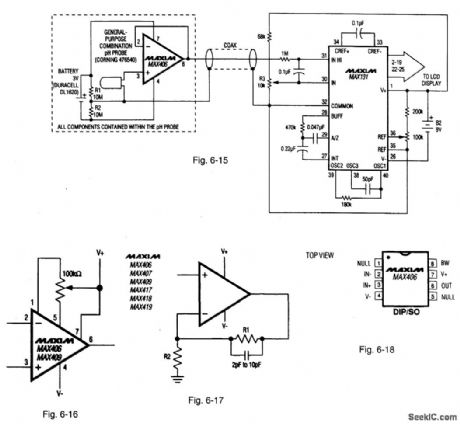
Figure 6-15 shows a MAX406 combined with a MAX131 ADC to form a buffered pH probe. This circuit eliminates expensive low-leakage cables that often connect pH probes to meters. The MAX406 and a lithium battery are included in the probe housing. A conventional low-cost cable carries the buffered pH signal to the MAX131. In most cases, the 3-V battery life exceeds the functional life of the probe.Figures 6-16, 6-17, and 6-18 show the offset-voltage adjustment, feedback compensation, and pin configurations, respectively for the MAX406. Notice that the feedback compensation (Fig. 6-17) is not required in all cases. MAXIM NEW RELEASES DATA Book, 1993, P. 3-5, 3-28, 3-29. (View)
View full Circuit Diagram | Comments | Reading(2087)
Traditional op-amp inverting attenuator circuit
Published:2011/7/28 4:16:00 Author:John | Keyword: op-amp, inverting attenuator
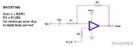
Traditional op-amp inverting attenuator circuit is shown.
(View)
View full Circuit Diagram | Comments | Reading(2401)
Addition and subtraction counter within 100 circuit
Published:2011/7/28 4:14:00 Author:John | Keyword: Addition and subtraction counter

Addition and subtraction counter within 100 circuit is shown.
(View)
View full Circuit Diagram | Comments | Reading(970)
| Pages:1242/2234 At 2012411242124312441245124612471248124912501251125212531254125512561257125812591260Under 20 |
Circuit Categories
power supply circuit
Amplifier Circuit
Basic Circuit
LED and Light Circuit
Sensor Circuit
Signal Processing
Electrical Equipment Circuit
Control Circuit
Remote Control Circuit
A/D-D/A Converter Circuit
Audio Circuit
Measuring and Test Circuit
Communication Circuit
Computer-Related Circuit
555 Circuit
Automotive Circuit
Repairing Circuit