
Circuit Diagram
Index 1260
1_W_CLASS_B
Published:2009/6/28 23:42:00 Author:May

Audio application of CA3020A wideband power amplifier provides 1-W outputto loudspeaker load through AF output transformer with 10% total harmonic distortion VCC1 is 9 V、and VCC2 is 12 V With CA3020 both supply voltages are 9V and maximum power output is 550 mW.Sensitivity is 35-45 mV,-″Linear Integrated Circuits and MOS/FET's,″RCASolid State Division,Somelville, NJ, 1977,p 105 (View)
View full Circuit Diagram | Comments | Reading(948)
Adjustable_dc_dc_step_down_converer2A
Published:2009/7/25 1:10:00 Author:Jessie
This circuit shows an LAS-6320P used as a step-down converter with an adjustable output. (View)
View full Circuit Diagram | Comments | Reading(633)
MICROVOLT_COMPARATOR
Published:2009/6/28 23:42:00 Author:May
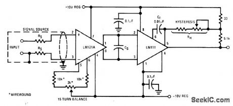
Combination of National LM121A preamp and LM111 comparator serves for comparing DC signal levels that are only within microvolts of each other. With bias network shown, preamp has open-loop temperature-stable voltage gain close to 100.Separation of preamp from comparator chip minimizes effects of temperature variations.Circuit hysteresis is 5 μV, which under certain conditions can be trimmed to 1 μV.— Linear Applications, Vol. 2, National Semiconductor, Santa Clara, CA, 1976, LB-32. (View)
View full Circuit Diagram | Comments | Reading(1257)
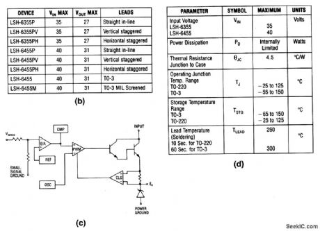
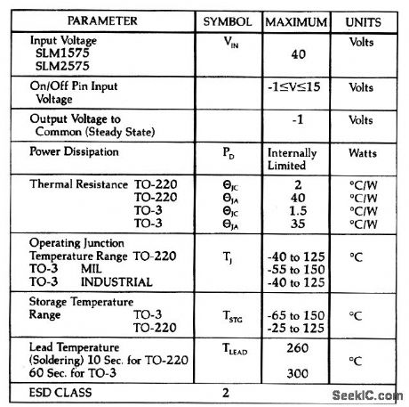
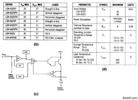
_8_A_dc_dc_step_down_converter
Published:2009/7/25 1:09:00 Author:Jessie
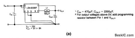
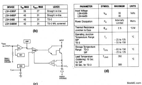
The LSH switching-regulator ICs contain most elements necessary for converter operation, as shown in Fig. 4-6C. Figure 4-6B shows the output voltage and characteristics for various part numbers. Figure 4-6D shows the absolute maximum ratings. Simply add a choke, catch diode, and two capacitors to the IC for a complete converter. (View)
View full Circuit Diagram | Comments | Reading(640)
HEADPHONE_OPAMPS
Published:2009/6/28 23:42:00 Author:May
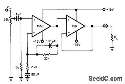
Dual low-noise 4558 opamp provides gain and reduces system noise and distortion, while 759 power opamp supplies output power of 0.7 W into 16-ohm load with Iessthan 0.170 total harmonicdistortion.-R. J. Apfel, Power Op Amps-Their Innovative Circuits and Packaging Provide Designers with More Options, EDN Magazine, Sept.5,1977, p 141-144. (View)
View full Circuit Diagram | Comments | Reading(4474)
OTA_single_control_function_generatorminimum_component
Published:2009/7/25 1:09:00 Author:Jessie
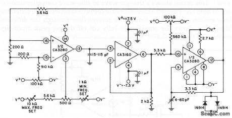
This circuit is similar to that of Fig.11-3,except that less components(and adjustments) are required.The frequency range is from 2 Hz to 1 MHz. (View)
View full Circuit Diagram | Comments | Reading(860)
HIGH_SPEED_LASER_DIODE_DRIVER
Published:2009/6/28 23:41:00 Author:May
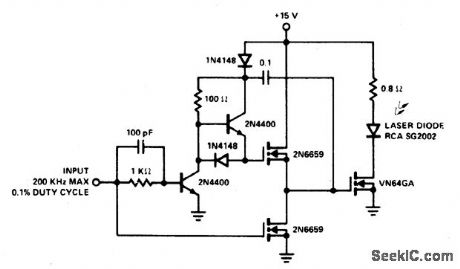
Circuit NotesA faster driver, can supply higher gate current to switch the VN64GA very quickly. The circuit uses a VMOS totemple, stage to drive the high power switch. (View)
View full Circuit Diagram | Comments | Reading(1510)
Differential_to_single_ended_converter
Published:2009/7/25 1:07:00 Author:Jessie
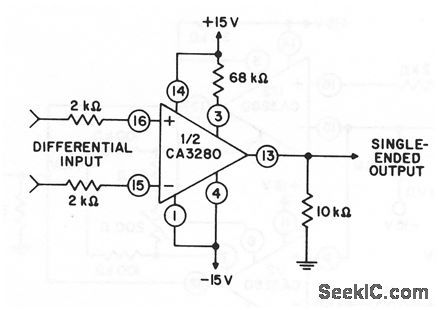
This circuit shows one section of an OTA connected to provide a single-ended output for a differential input. (View)
View full Circuit Diagram | Comments | Reading(1608)
TACHOMETER
Published:2009/6/28 23:40:00 Author:May
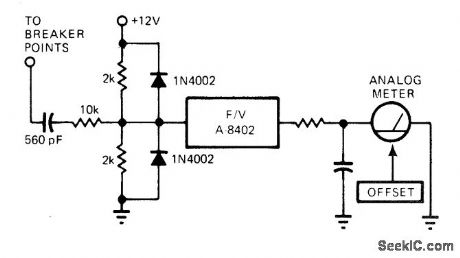
Intech/Function Modules A-8402 operating in frequency-to-vol tage converter mode serves as automotive tachometer having inherent linearity and ease of calibra-tion. Convener operates asynchronously, which does not affect accuracy when driving analog meter.-P. Pinter and D. Timm, Voltage-to-Frequency Converters-IC Versions Perform Accurate Data Conversion (and Much More) at Low Cost, EDNMagazine, Sept. 5, 1977, p 153-157. (View)
View full Circuit Diagram | Comments | Reading(0)
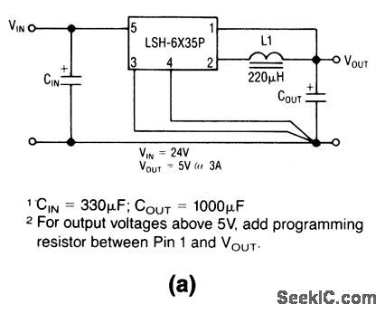
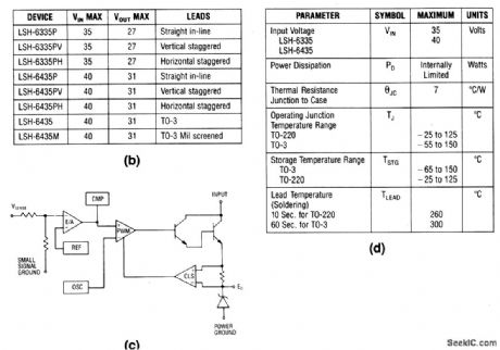
5_A_dc_dc_step_down_converter
Published:2009/7/25 1:07:00 Author:Jessie

The LSH switching-regulator ICs contain most elements necessary for converter operation, as shown in Fig. 4-5C. Figure 4-5B shows the output voltage and characteristics for various part numbers. Figure 4-5D shows the absolute maximum ratings. Simply add a choke, catch diode, and two capacitors to the IC for a complete converter. (View)
View full Circuit Diagram | Comments | Reading(800)
STROBED_COMPARATOR
Published:2009/6/28 23:39:00 Author:May
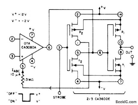
Combination of CA3080A opamp and two CMOS transistor pairs from CA3600E array gives programmable micropower comparator having quiescent power drain of about 10μW. When comparator is strobed on, opamp becomes activeand circuit draws 420μW while responding to differentialinput signalin about 8μs. Common-mode input range is -1 V to +10.5 V. Voltage gain of comparator is typically 130 dB.— Linear Integrated Circuits and MOS/FET's, RCA Solid State Division, Somerville, NJ, 1977, p 279. (View)
View full Circuit Diagram | Comments | Reading(843)
3_A_dc_dc_step_dowm_converter
Published:2009/7/25 1:04:00 Author:Jessie
The LSH switching-regulator ICs contain most elements necessary for converter operation, as shown in Fig. 4-4C. Figure 4-4B shows the output voltage and characteristics for various part numbers. Figure 4-4D shows the absolute maximum ratings. Simply add a choke, catch diode, and two capacitors to the IC for a complete converter. (View)
View full Circuit Diagram | Comments | Reading(701)
LOW_EMISSION_CD
Published:2009/6/28 23:38:00 Author:May
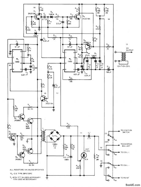


Solid-state capacitor-discharge ignition system improves combustion efficiency by increasing spark duration. For 8-cylinder engine, normal CD system range of 180 to 300,ttS is increased to 600 ps below 4000 rpm the discharge lasts for one cycle or 300 pts because at higher speeds the power cycle has shorter times. Circuit uses 555 timer M1 as 2-kHz oscillator, with Q1-Q3 providing drive to Q4-Q5 and T, for converting battery voltage to about 400 VDC at output of bridge rectifier. When dis-tributor points open,Q7 turns on and triggers M2 connected as mono that provides gate drive pulses for SCR. Article describes operation of circuh in detail and gives waveforms at points a-i.-C. C. Lo, CD lgnition System Produces Low Engine Emissions, EDN Magazine, May 20, 1976, p 94, 96, and 98. (View)
View full Circuit Diagram | Comments | Reading(2142)
SUPPRESSING_OSCILLATION
Published:2009/6/28 23:36:00 Author:May
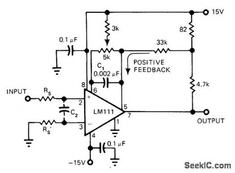
Use of positive feedback to pin 5 of comparatorgives sharp and clean output transitions even with slow triangle-wave inputs, with no possibility of comparator bursting into oscillation near crossing point. Input resistors should not be wirewound.Circuit will handle triangle-wave inputs up to several hundred kilohertz.—P. Lefferts, Overcome Comparator Oscillation Through Use of Careful Design, EDN Magazine, May20, 1978, p 123-124. (View)
View full Circuit Diagram | Comments | Reading(755)
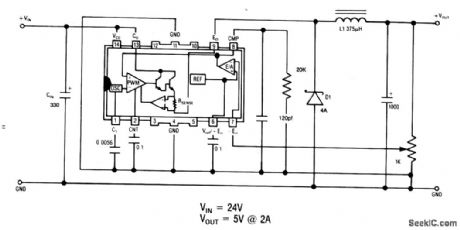
2_A_dc_dc_step_down_converter
Published:2009/7/25 1:00:00 Author:Jessie
The LSH switching-regulator ICs contain most elements necessary for converter operation, as shown in Fig. 4-3C. Figure 4-2B shows the output voltage and characteristics for various part numbers. Figure 4-3D shows the absolute maximum ratings. Simply add a choke, catch diode, and two capacitors to the IC for a complete converter. (View)
View full Circuit Diagram | Comments | Reading(591)
High_Q_notch_filter
Published:2009/7/25 0:44:00 Author:Jessie
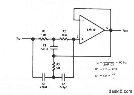

This circuit uses an LM110 connected to form a basic high-Q notch filter. The frequency range is determined by the values of R1 and C1, as shown by the equation. National Semiconductor, Linear Applications Handbook, 1991, p. 1202. (View)
View full Circuit Diagram | Comments | Reading(2137)
Bell Signal Generator Circuit
Published:2011/7/21 0:49:00 Author:Joyce | Keyword: Bell, Signal , Generator
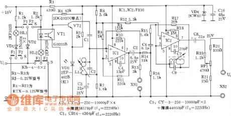
Bell signal generator is usually a calling signal source for communication equipment. Under the control of the automatic exchange system, oscillator for sending the call will produce frequency shift calling signals for the user to choose the one needs calling. The bell signal generator is composed of frequency shift control circuit, LC frequency shift oscillator and output circuit as shown in the figure.
(View)
View full Circuit Diagram | Comments | Reading(663)
Norton_positive_feedback_oscillator
Published:2009/7/25 1:39:00 Author:Jessie
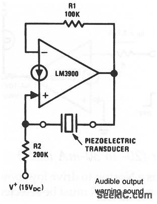
This circuit shows a Norton used as a driver for a piezoelectric transducer (a warning type of noise maker). The output is returned back to the (+) terminal through the transducer to sustain oscillation (at the resonant frequency determined by the transducer). Resistors R1 and R2 bias the output voltage at V+/2 to keep the amplifier in the active region. (View)
View full Circuit Diagram | Comments | Reading(1764)
Dual_output_transformerless_converter
Published:2009/7/25 1:39:00 Author:Jessie
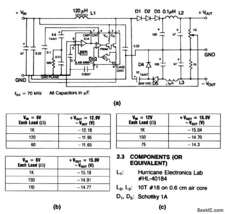
This circuit provides a dual output without transformers. Typical performance and component source information are shown in Figs. 4-30B and 4-30C, respectively. (View)
View full Circuit Diagram | Comments | Reading(797)
555 bipolar power conversion circuit
Published:2011/7/21 3:09:00 Author:Ecco | Keyword: 555, bipolar, power conversion
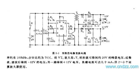
As shown in Figure 9-3, the conversion circuit includes the pulse oscillator and bipolar rectifier circuit. It is used to transfer a group of power supply into two groups of ± 12V DC voltage source in digital circuits and analog mixed circuit board with op amp. The circuit can no longer be set two voltage sources. 555 and R1, R2, C3 form a multivibrator which is in non-steady state, the oscillation frequency f = 1.44 / (R1 +2 R2) C3, the frequency of the icon parameter is about 100kHz, duty cycle is about 70%; the other way gets + 12V voltage. Load current can be up to tens of mA for 2 to 3 op amps.
(View)
View full Circuit Diagram | Comments | Reading(1777)
| Pages:1260/2234 At 2012411242124312441245124612471248124912501251125212531254125512561257125812591260Under 20 |
Circuit Categories
power supply circuit
Amplifier Circuit
Basic Circuit
LED and Light Circuit
Sensor Circuit
Signal Processing
Electrical Equipment Circuit
Control Circuit
Remote Control Circuit
A/D-D/A Converter Circuit
Audio Circuit
Measuring and Test Circuit
Communication Circuit
Computer-Related Circuit
555 Circuit
Automotive Circuit
Repairing Circuit