
Circuit Diagram
Index 1247
BOUNCELESS_ISOLATOR
Published:2009/6/29 3:48:00 Author:May

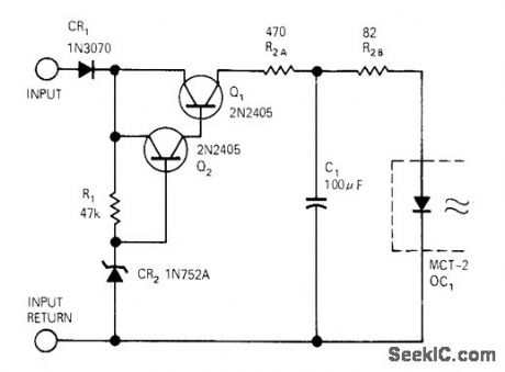
Integrating filter C1-R2 eliminates effects of contact bounce that may be superimposed on digital input signal feeding optoisolator. Photodiode in optoisolator drives Schmitt trigger that makes output to TEL circuits change state when LED is turned on by input signaL—C. E. Mitchell, Optical Coupler and Level Shifter, EDN|EEE Magazine, Feb.1, 1972, p 55. (View)
View full Circuit Diagram | Comments | Reading(750)
ONE_PULSE_PER_PUSH
Published:2009/6/29 3:47:00 Author:May
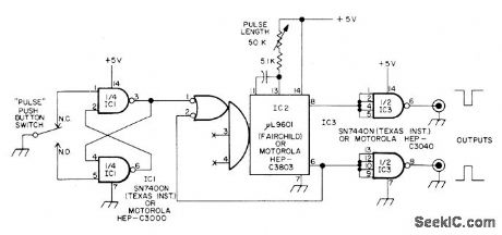
Circuit generates only one rectangular pulse for each actuation of pushbutton switch, even if contacts bounce.TTL gates IC1 are wired as RS flip-flop (latch) that triggers mono MVBR IC2 having fixed-duration positive and negative output pulses.Output drives are increased by TTL inverting buffer gates.—H. Olson, Further Adventures of the Bounceless Switch, 73 Magazine, Feb. 1975, p 111-114. (View)
View full Circuit Diagram | Comments | Reading(1284)
Protective principle circuit diagram
Published:2011/8/1 2:23:00 Author:Ecco | Keyword: Protective principle
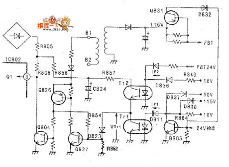
Protective circuitry: According to figure 1, when the supply is in start state, the electricity can be connected by R805, R858. On the one hand, when the output voltage is rising, the D811 can reach the state of starting by the IF1 of R864. D836 is later than D811, it appears the state of start when the current flows to LF2 from F, B, T 24. Then, IF1 produces firstly, IF2 is later, after Tr1 appears the state of ON , Tr2 can be switched on. When the burden is unusual, for example, it can produce overcurrent, and when base current of Q805 produces, Q805 appears the state of ON . When IF1 of D811 is cut-off, Tr1 will be the state of OFF . Q827 appears the state of breakover by VTr1 when through D823. Simultaneously, Q826 is also in starting state. The collector current Ic make the Q804 is in staring state, and the shunt of Ic passes R854 that make of Q827 base maintaining current, Q827, Q826 keep in the staring state. With the Ic, Q804 is in the staring state, the base of Q1 locating inside of IC802 connects 3 and then connects to the earth, the supply will stop working. When appearing short circuit, the circumstances are as below: a. 50V short circuit: D837 is on, D811 is stop. b. 115V short circuit: D830 is on, D811 is stop. c. 16V short circuit: the current of D811 isn't provided by R864, D811 will stop.
(View)
View full Circuit Diagram | Comments | Reading(539)
Four_cell_NiCad_power_management
Published:2009/7/24 22:47:00 Author:Jessie
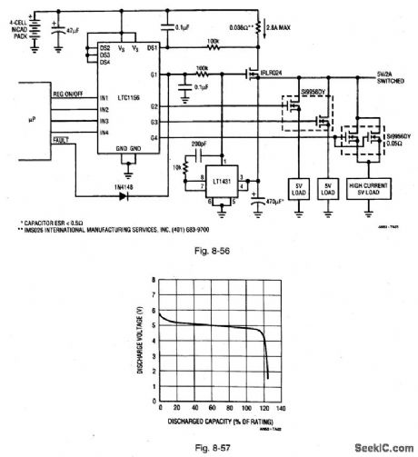
Figure 8-56 shows one channel of an LTC1156 used to regulate the output of a four-cell NiCad battery pack to power a notebook or palmtop computer. Figure 8-57 shows typical four-cell NiCad discharge charaqteristics. As long as the input voltage to the regulator is sufficient to produce 5 V at the output, the regulator limits at 5 V. When the battery-pack voltage drops below 5 V, the MOSFET is fully enhanced, and acts as a direct connection between the battery and the computer circuits. A battery-voltage monitor in the microprocessor decides when the battery voltage drops below 4.6 V, and housekeeping is performed (data storage, etc.) before the batteries are completely discharged. The other three channels of the LTC 1156 act as switches (under microprocessor control) to power the remaining sections of the computer. The number of switches can be increased by adding more LTC1155 or LTC1156 circuits as needed. LINEAR TECHNOLOGY, APPLICATION NOTE 53, P. 11.
(View)
View full Circuit Diagram | Comments | Reading(717)
REMOTE_ON_OFF_SWITCH
Published:2009/6/29 3:47:00 Author:May
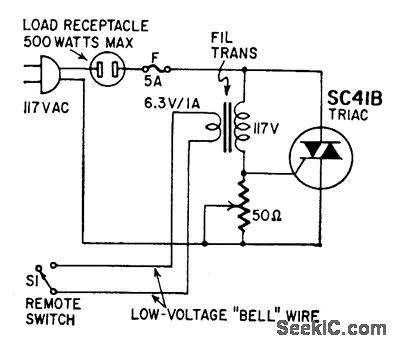
This circuit provides power control with-out running line-voltage switch leads. The primary of a 6-volt filament transformer is con-nected between the gate and one of the main terminals of a triac. The secondary is connected to the remote switch through ordinary low-voltage line. With switch open, transformer blocks gate current, prevents the triac from firing and applying power to the equipment. Closingthe switchshort-circuits the secondary, causing the transformer to saturate and trigger the triac. (View)
View full Circuit Diagram | Comments | Reading(1190)
Op_amp_differentictl_input_instrumentation_amplifier
Published:2009/7/24 22:45:00 Author:Jessie
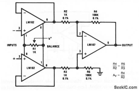
This is the op-amp version of the classic instrumentation amplifier.The circuit provides 10-V output for a 100-mW input, with gain set by the ratio of R4/R2 and R5/R3, while rejecting ±11V of common-mode noise. With both inputs grounded, R1 is adjusted until the output is zero. (View)
View full Circuit Diagram | Comments | Reading(856)
1_W_INVERTING
Published:2009/6/29 3:11:00 Author:May
Uses Motorola MC1554 power amplifier to provide voltage gain of 35 with componentsshown. Output voltageswing is 12 V P-P into 12-ohm load. For responsedown to low audio frequencies (below 100 Hz), large value of C is required, such as 1μF. Input can be direct-coupled at sacrifice in output offset, but this can be corrected by properly biasing pin 1 or terminating it in about 250 ohms. Upper fre-quency limit for -3 dB is about 22,000 Hz.-' The MC1554 One-Watt Monolithic Integrated Circuit Power Amplifier, Motorola, Phoenix, AZ, 1972, AN.401, p 3. (View)
View full Circuit Diagram | Comments | Reading(691)
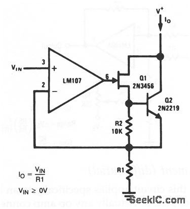
Precision_current_source
Published:2009/7/24 22:43:00 Author:Jessie
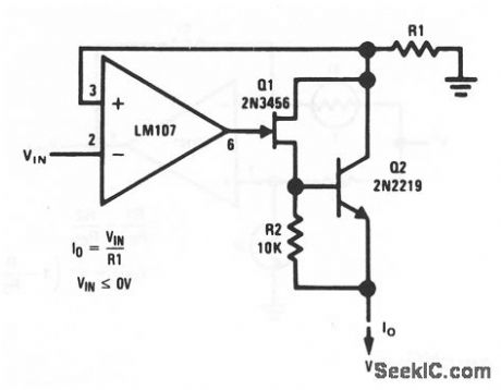
The output of this circuit depends on VIN and the value of R. Notice that VIN can be anything from 0 to (V- +1 V) and V- can be -2 to -35 V. (View)
View full Circuit Diagram | Comments | Reading(0)
Low Frequency Oscillation Circuit(Luminescent Circuit ) Based on 555 Time-base Circuit
Published:2011/7/22 2:32:00 Author:Joyce | Keyword: Low Frequency, Oscillation , 555 Time-base
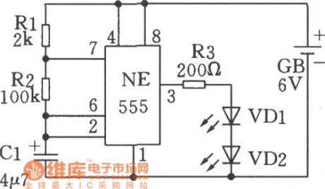
As shown in the figure is a luminescent circuit, in which the two leds will flicker simultaneously under proper functioning. Principle of this circuit is similar to that of 555 audio oscillator ,the difference between them is that the capacity of the capacitance C1 will increase to 4.7μ F. Therefore, the oscillation frequency of the circuit is very low, and the changing speed of the level of feet 3 of NE555 will slow down. When feet 3 outputs a high level, led VD1 and VD2 will be on and flicker. When feet 3 outputs a low level, the two leds will go out. (View)
View full Circuit Diagram | Comments | Reading(745)
45_W_CLASS_B
Published:2009/6/29 3:08:00 Author:May
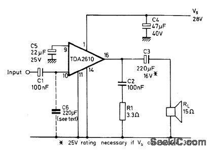
Mullard TDA2610 drives 15-ohm loudspeaker with total harmonic distor-tion of lessthan 1%. Supply is 28V ±10%. Net-work C2-R1 ensures stability with inductive Ioad.- Audio Power Amplifier TDA2610, Mullard, London, 1976, Technical Note 35, TP1541. (View)
View full Circuit Diagram | Comments | Reading(1204)
FEED_FORWARD_CORRECTION
Published:2009/6/29 3:05:00 Author:May
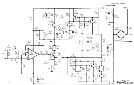
Circuit re-duces distortion caused by nonlinearity of out-put power transistors by deriving error com ponent that bypasses these transistors.Technique used is known as current dumping.Article describes operating principle in detail.Circuit shown gives application to commercial amplifier (Quad 405), in which midfrequency distortion is only about 0.005%. Features in-clude elimination of adjustments, alignment procedures and thermal problems during entire life of amplifier,-P.J. Walker, Current Dumping Audio Amplifier,Wireless World,Dec.1975,p 560-562 (View)
View full Circuit Diagram | Comments | Reading(2225)
Precision_current_sink
Published:2009/7/24 22:41:00 Author:Jessie
As shown,the ability of this circuit to sink current depends on VIN and the value of R1. Note that VIN can be anything from 0 to (V+-1V), and can be +2 to +25 V. (View)
View full Circuit Diagram | Comments | Reading(1)
DEBOUNCER
Published:2009/6/29 2:57:00 Author:May
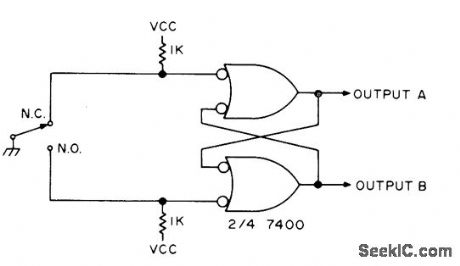
Generates single pulse on switch closure, provided wiper of switch bounces only between contact and an open. Output A goes low when switch is pushed, and at same time output B goes high.—E. E. Hrivnak, House Cleaning the Logical Way, 73 Magazine, Aug. 1974, p 85-90. (View)
View full Circuit Diagram | Comments | Reading(937)
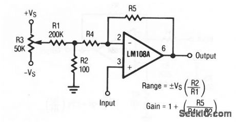
Op_amp_offset_adjustment_inverting
Published:2009/7/24 22:39:00 Author:Jessie
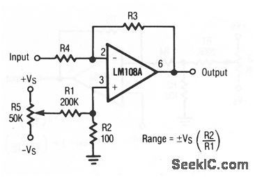
Although this circuit applies specifically to an LM108A, the values and equations can be adapted to virtually any op amp connected in the inverting configuration. (View)
View full Circuit Diagram | Comments | Reading(721)
12_W_OUTPUT
Published:2009/6/29 2:55:00 Author:May
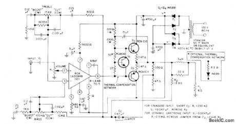
Uses CA3094B programmable opamp to drive complementary- symmetry power-output transistors. Intermodulation distortion is only 0.2% when 60-Hz and 2-kHz signals are mixed in 4:1 ratio. Location of tone con| trols in feedback network improves signal-to-noise ratio. Hum and hoise are typically 700μV (83 dB down) at output. Transistor Q1 provides thermal compe"sation,-″Circuit Ideas for RCALinear ICs、″RCA Solid Stat Divsion、Somerville NJ、1977、p 11 (View)
View full Circuit Diagram | Comments | Reading(712)
5_W_WITH_OPAMP
Published:2009/6/29 2:54:00 Author:May
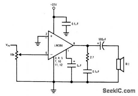
Simple circuit including volume control has low harmonic distortion.Higher allowable operating voltage of LM384 opamp gives higher output power, but heatsink is required.- Audio Handbook, National Semiconductor, Santa Clara, CA, 1977, p 4-28-4-29. (View)
View full Circuit Diagram | Comments | Reading(891)
Op_amp_offset_adjustment_differential
Published:2009/7/24 22:20:00 Author:Jessie
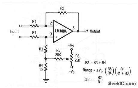
Although this circuit applies specifically to an LM108A, the values and equations can be adapted to virtually any op amp connected in the differential-input configuration. (View)
View full Circuit Diagram | Comments | Reading(1524)
ERROR_ADD_ON_REDUCES_DISTORTION
Published:2009/6/29 2:54:00 Author:May
Based on fact that error at output of upper opamp also appears at input of this opamp, Error signal is taken from this input for lower opamp, where it is amplified by opamp and Darlington for addition to output of upper Darlington. Article gives design equations and intimates that open-loop gain improves at 12 dB per octave as compared to conventional 6 dB, Applications include reduction of loudspeaker distortion which cannot be handled by negative feedback.-A.Sandman, Reducing Distortion by 'ErrorAdd-On.' Wireless World, Jan. 1973, p 32. (View)
View full Circuit Diagram | Comments | Reading(782)
Low Frequency Oscillation Circuit(Luminescent Circuit ) Based on 555 Time-base Circuit Two
Published:2011/7/22 2:47:00 Author:Joyce | Keyword: Low Frequency, Oscillation , 555 Time-base
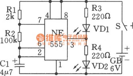
As shown in the figure is a flasher circuit centering on 555 circuit .LED VD1 and VD2 will flicker alternately under proper functioning. Principle of the circuit is briefly described as follows: Time base circuit NE555 and R1, R2, C1 compose the low frequency oscillator. After the circuit starts oscillation, the level of feet 3 of time base circuit 555 will change. When feet 3 is high level, VD1 will be cut off and it will not flicker, but VD2 will. When feet 3 is low level, VD1 will be on and flicker ,while VD2 will be cut off and stop flickering .So,the two leds will flicker alternatively. Colors of the two LEDs should be red, green or yellow since it would make the difference more obvious.
(View)
View full Circuit Diagram | Comments | Reading(573)
Op_amp_offset_adjustment_noninverting
Published:2009/7/24 22:19:00 Author:Jessie
Although this circuit applies specifically to an LM108A, the valuesand equations can be adapted to virtually any op amp connected In the noninverting configuration. (View)
View full Circuit Diagram | Comments | Reading(806)
| Pages:1247/2234 At 2012411242124312441245124612471248124912501251125212531254125512561257125812591260Under 20 |
Circuit Categories
power supply circuit
Amplifier Circuit
Basic Circuit
LED and Light Circuit
Sensor Circuit
Signal Processing
Electrical Equipment Circuit
Control Circuit
Remote Control Circuit
A/D-D/A Converter Circuit
Audio Circuit
Measuring and Test Circuit
Communication Circuit
Computer-Related Circuit
555 Circuit
Automotive Circuit
Repairing Circuit