
Circuit Diagram
Index 1254
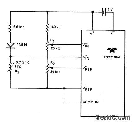
BASIC_DIGITAL_THERMOMETER_CELSIUS_AND_FAHRENHEIT_SCALES
Published:2009/6/29 2:02:00 Author:May
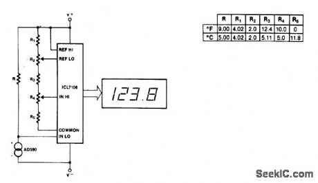
Maximum reading on the Celsius range is 199.9 ℃, limited by the (short-term) maximum allowable sensor temperature. Maximum reading on the Fahrenheit range is 199.9 °F (93.3 ℃), limited by the number of display digits. VREF for both scales is 500 mV. (View)
View full Circuit Diagram | Comments | Reading(1349)
SLEW_RATE
Published:2009/6/29 2:01:00 Author:May
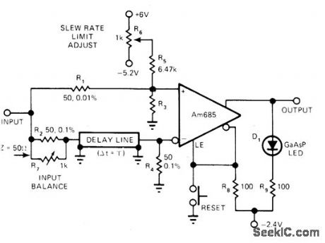
Circuit measures slew rate of input signal with Am685 comparator in circuit having delay-line length under 10 ns. When slew rate exceeds predetermined Iimit set by R6, comparator changes state and latches, turning on LED. Pushing reset switch restores normal operation. Based on comparison of input signal with time-delayed counterpart. Derivative of input signal, equal to its instantaneous slew rate, is measured accurately for swings of 6 V P-P as found in most 50-ohm video signals. Action is fast enough to detectglitches.—R. C. Culter, Slew-Rate Limit Detector is Simple, yet Versatile, EDN Magazine, Aug. 20, 1977, p 140-141. (View)
View full Circuit Diagram | Comments | Reading(1696)
FREQUENCY_COMPARATOR
Published:2009/6/29 2:01:00 Author:May
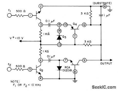
Circuit using CA3096 transistor amay plus one discrete diode develops DC output voltage that is proportional to difference between frequencies of input signals f1 and f2. Maximum input frequency is 10 kHz.— Circuit Ideas for RCA Linear ICs, RCA Solid State Division, Somerville, NJ, 1977, p 17. (View)
View full Circuit Diagram | Comments | Reading(1382)
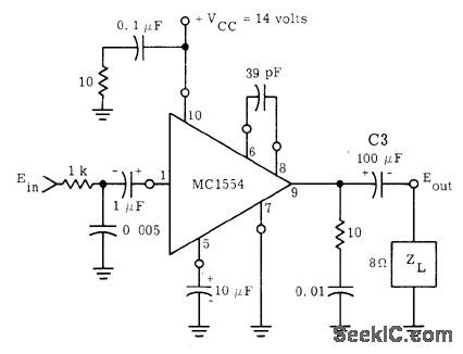
1_W_NONINVERTING_WITH_SPLIT_SUPPLY
Published:2009/6/29 2:00:00 Author:May
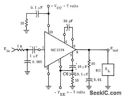
Motorola MC1554 IC is connected for operation from ±7 V to provide voltage gain of 9 overfre。quency range(-3 dB)of 40 to 22,000 Hz,Inputimpedanceis 10K,and total harmonic distortionis is less than 0.75%, Use external heatsink,-″The MC1554 One-Watt Monolithic Integrated Circtiit Power AmpIifier, Motorola、 Phoenix,AZ,1972、AN-401、p 2 (View)
View full Circuit Diagram | Comments | Reading(796)
POSITIVE_TEMPERATURE_SENSOR_COEFFICIENT_RESISTOR
Published:2009/6/29 2:00:00 Author:May
View full Circuit Diagram | Comments | Reading(1047)
FIBER_OPTIC_RECEIVER,VERY_HIGH_SENSITIVITY,LOW_SPEED,3nW
Published:2009/6/29 2:00:00 Author:May
View full Circuit Diagram | Comments | Reading(642)
1_W_NONINVERTlNG
Published:2009/6/29 2:00:00 Author:May
Motorola MC1554 IC operates from single supply and uses capacitive coupling to both source and load, for voltage gain of 9 with frequency response (-3 dB) from 200 to 22,000 Hz. Input impedance is 10K, and total harmonic distortion is Iess than 0.75%.Use external heatsink.- The MC1554 One-Watt Monolithic Integrated Circuit Power Am-plifier, Motorola, Phoenix, AZ, 1972, AN-401, p 2. (View)
View full Circuit Diagram | Comments | Reading(764)
5_W_CLASS_A
Published:2009/6/29 2:00:00 Author:May
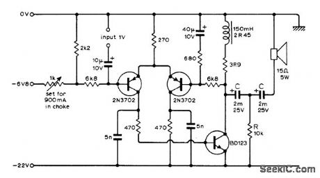
Three-transistor feedback loop gives excellent DC stability, while arrangement of two capacitors and resistor feeding loudspeaker keeps these capachors properly polarized as AF output voltage swings above and below zero Ievel.-R. H. Pearson, Novel 5-Watt Class A Amplifier Uses Three-Transistor Feed-back Circuit, Wl'reless World, March 1974, p 18. (View)
View full Circuit Diagram | Comments | Reading(928)
GROUND_REFERRED_CENTIGRADE_THERMOMETER_1
Published:2009/6/29 1:59:00 Author:May
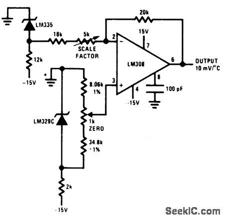
View full Circuit Diagram | Comments | Reading(1910)
LOW_NOISE_TRANSFORMERLESS_PREAMP
Published:2009/6/29 1:59:00 Author:May
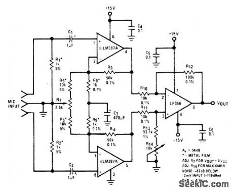
Noise performance of balanced microphone preamp is improved with instrumentation amplifier configuration of three opamps. Each half of LM387A is wired as noninverting amplifier.LM387A serves to amplify low-level signals VOUT while adding as little noise as possible, leaving common-mode rejection for LF356.- Audio Handbook, National Semiconductor, Santa Clara, CA, 1977, p 2-37-2-40. (View)
View full Circuit Diagram | Comments | Reading(4131)
INDEPENDENT_HYSTERESIS_ADJUSTMENT
Published:2009/6/29 1:59:00 Author:May
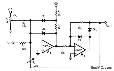
Trip point and hysteresis of comparator opamp A1 can be adjusted independently, with trip point being determined by setting of R1 or programmed by DC voltage applied to R2. Opamp A2 provides polarity inversion and rectification of A2 output. Hysteresis control R8 is in feedback path from A2 back to A1. Amount of hysteresis is determined by ratio of R3 to R8. With values shown, circuit output levels are 0 and 5 V.—G.Tobey, Comparator with Noninteracting Adjustments, EDN|EEE Magazine, Oct, 1, 1971, p 43. (View)
View full Circuit Diagram | Comments | Reading(826)
TEMPERATURE_SENSOR_1
Published:2009/6/29 1:58:00 Author:May
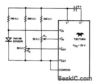
View full Circuit Diagram | Comments | Reading(1012)
ZENEB_REFERENCE
Published:2009/6/29 1:58:00 Author:May
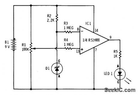
One section of RS3900 quad opamp is connected as comparator using zener D1 for reference voltage. When voltage applied to pin 13 by R1 exceeds breakdown voltage of zener D1, comparator amplifies difference voltage to produce output voltage high enough to turn on LED. Can be used for classroom demonstration of comparator action.Zener breakdown should be under 9 V. LED can be Radio Shack 276-041.—F. M. Mims, Semiconductor Projects, Vol. 2, Radio Shack, Fort Worth, TX, 1976, p 35-42. (View)
View full Circuit Diagram | Comments | Reading(776)
FIBER_OPTICS_HALF_DUPLEX_INFORMATION_LINK
Published:2009/6/29 1:58:00 Author:May
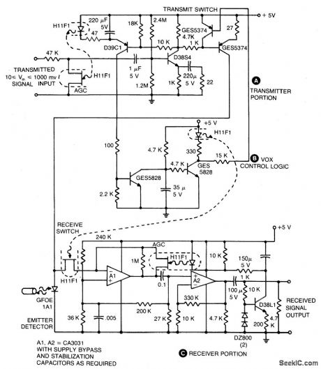
View full Circuit Diagram | Comments | Reading(702)
Low_dropout_linear_regulator
Published:2009/7/25 4:21:00 Author:Jessie
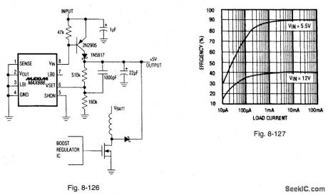
Figure 8-126 shows a MAX666 linear regulator connected to provide a 5-V output. This circuit is useful for uninterruptible battery-backup applications, as well as forlow-power circuits that use batteries for maln power and optionally take powerfrom wall-cube ac adapters.The input-voltage range is 5.4 V to 16.5 V, quiescent current(VIN =10 V) is 20 μA, dropout voltage (with 100-mA load) is 400 mV,maximum load current (VIN=6 V) is 500 mA and shutdown current is 5 μA,Figure 8-127 shows the efficiency curves.Notice that the pass transistor is externaland can be sized to handle the required power dissipation.If the dissipation is lowenough the MAX666 internal 50-mA power transistor can replace the 2N2905.TheMAX667 should also be considered In such cases. (The MAX667 has a larger, 250-mA pass transistor and lower dropout voltage.) MAXIM BATTERY MANAGEMENT CIRCUIT COLLECTION, 1994, P. 74.
(View)
View full Circuit Diagram | Comments | Reading(902)
GROUND_REFERRED_CENTIGRADE_THERMOMETER
Published:2009/6/29 1:57:00 Author:May
View full Circuit Diagram | Comments | Reading(930)
IC_precision_waveform_generator_with_variade_duty_cycle
Published:2009/7/25 4:21:00 Author:Jessie
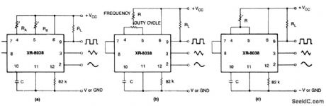
These circuits are similar to that of Fig 5-47,exceptfor alternate timing configurations and a duty-cycle control, If two separate timing resistors are used (Fig. 5-48A), the output frequency is: f= 0.3/RC, where RA= RB = R. If one timing resistor is used (Fig. 5-48B or 5-48C), the output frequency is: f =0.15/RC. If the duty cycle is to be varied over a small range, it should be centered around a duty cycle of 50%. (View)
View full Circuit Diagram | Comments | Reading(2104)
GROUND_REFERRED_FAHRENHEIT_THERMOMETER
Published:2009/6/29 1:55:00 Author:May
View full Circuit Diagram | Comments | Reading(1119)
IC_precision_waveform_generator
Published:2009/7/25 4:19:00 Author:Jessie


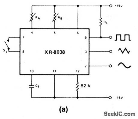


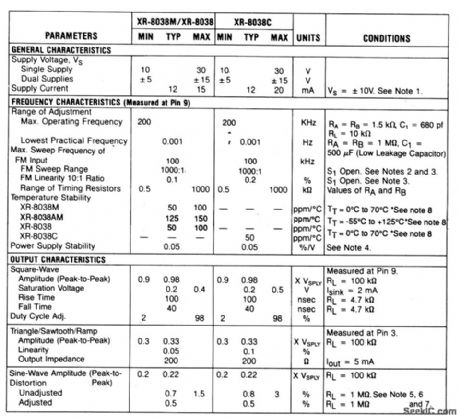
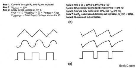
This circuit uses an XR-8038 to provide simultaneous sine, square, and triangle outputs, which can be sweep and frequency odulated,The frequency range is from 0.001 Hz to 200 kHz、with a variable duty cycle from 2%to 98% Electrical characteristics、and phase relationships of the outputs, are shown in Figs.5-47B and 5-47C,respectively.The operating frequency is set by capacitor C at pin 10,and the timing resistors at pins 4 and 5 See Conditions in Fig.5-47B. (View)
View full Circuit Diagram | Comments | Reading(1729)
0℃_100℃_THERMOMETER
Published:2009/6/29 1:55:00 Author:May
View full Circuit Diagram | Comments | Reading(825)
| Pages:1254/2234 At 2012411242124312441245124612471248124912501251125212531254125512561257125812591260Under 20 |
Circuit Categories
power supply circuit
Amplifier Circuit
Basic Circuit
LED and Light Circuit
Sensor Circuit
Signal Processing
Electrical Equipment Circuit
Control Circuit
Remote Control Circuit
A/D-D/A Converter Circuit
Audio Circuit
Measuring and Test Circuit
Communication Circuit
Computer-Related Circuit
555 Circuit
Automotive Circuit
Repairing Circuit