
Circuit Diagram
Index 1250
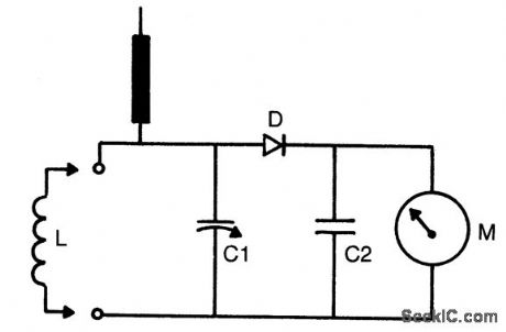
FIELD_STRENGTH_METER_15_to_150_MHz
Published:2009/6/29 2:28:00 Author:May
Circuit Notes
The tuning range is determined by coil (L) dimensions and setting of C1. Coils can be plugged in for multirange use or soldered in place if only limited frequency range is of interest. C1 = 36 pF variable, C2 =0047 disc, D = 1N60 (germanium) and M = 0-1 mA meter.For increased sensitivity, use 50μA meter. (View)
View full Circuit Diagram | Comments | Reading(645)
75_W_WITH_CURRENT_LIMITING
Published:2009/6/29 2:27:00 Author:May
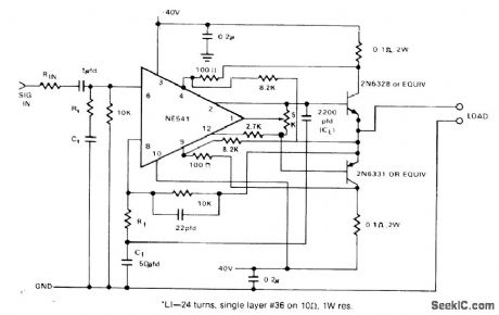

Signetics NE541 high-voltage power amplifier provides current gain of 90 dB from 20 Hz to 20 kHz andoutput levels up to 20 VRMS from 300-mVRMS input.IC includes built-in short-circuit protection,with additional protection provided by external current limiting,Transistors in output stage boost power to 75 W for driving loud-speaker load.- Signetics Analog Data Manual, Signetics, Sunnyvale, CA, 1977, p 765 (View)
View full Circuit Diagram | Comments | Reading(1338)
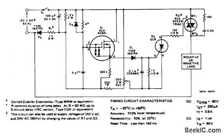
SOLID_STATE_TIMER_FOR_INDUSTRIAL_APPLICATIONS
Published:2009/6/29 2:27:00 Author:May

View full Circuit Diagram | Comments | Reading(984)
Automatic switching circuit of Multimeter AC to DC
Published:2011/7/17 23:12:00 Author:Sophia | Keyword: Automatic switching, Multimeter AC to DC
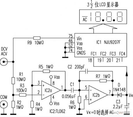
The AC and DC measurement conversion of ordinary digital multimeter is completed by manual operation. New digital multimeter DT860D adopts Automatic range switching chip NJU9207F, and is equiped with external auxiliary circuit to achieve AC - DC (AC / DC) automatic conversion measurements.
AC / DC automatic conversion circuit is shown below.
(View)
View full Circuit Diagram | Comments | Reading(2730)
High power adjustable regulated power supply using TL431
Published:2011/8/1 2:44:00 Author:Ecco | Keyword: High power , adjustable , regulated power supply
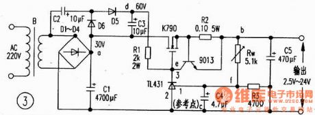
Precision voltage reference ICTL431 is T0-92 packaged, it is shown in Figure 1. Its performance is continuously adjustable output voltage being up to 36V, wide operating current range is 0.1. 100mA, the typical dynamic resistor is 0.22Ω, the output clutter is low. Figure 2 is a typical application of TL431, of which both ends of the output voltage of ③, ② feet V is 2.5 (R2 ten R3) V/R3. If you change the size of the resistance of R2, you can change the output voltage. Figure 3 uses it as external voltage reference and to drive the regulator FET K790, which makes output currentbe about 6A, the circuit is simple with safe power supply.The working principle
As Figure 3 shown, 220v voltage is stepped-down by the transformer B, rectified by D1-D4, filtered by C1. In addition, D5, D6, C2, C3 form double voltage circuit(making Vdc = 60V), Rw, R3 form voltage divider, T1431, R1 form sampling amplifier, 9013, R2 form limiting protection circuit, K790 FET tube is adjusting tube (which can be directly used in parallel), and C5 is the output filter circuit.
(View)
View full Circuit Diagram | Comments | Reading(4732)
Overvoltage charging protection circuit
Published:2011/7/30 10:09:00 Author:Sophia | Keyword: Overvoltage charging protection
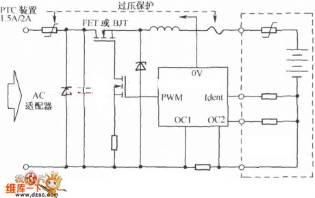
The effect of thermal components and the over-voltage protection components: they can provide current protection against over strong current which may damage the FET and current battery pack. When the polarity is inversed, the thermal components PTC will work to limit overcurrent. the overcurrent is generated by Zener diodes. When over-voltage components provide protection for the overloaded voltage by the components limiting the conduction current to acheive protection. (View)
View full Circuit Diagram | Comments | Reading(683)
Wien bridge sine wave generator composed of F007
Published:2011/8/1 2:43:00 Author:Ecco | Keyword: Wien bridge , sine wave , generator
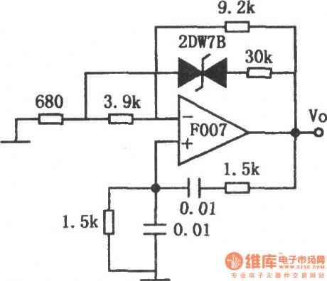
Figure shows the Wien bridge sine wave generator circuit. The regulator circuit is the Wien bridge oscillator circuit which is used to achieve steady increases, the oscillation frequency is 1kHz. If it uses coaxial double potentiometer to replace the l.5kΩ resistor of bridge, or changes the capacitor values by band switch, the output frequency can be adjusted. The highest frequency of the circuit is decided by the operational amplifier's frequency characteristics, while the low frequency side requires a larger resistance value, so the requirements of the op amp's input impedance should be as high as possible. Connecting in series with a 30kΩ resistor in a voltage-regulator tube branch, the branch is connected to between the 680Ω and 3.9kΩ resistor in order to make gain changes be not too fast. The use of soft breakdown characteristic regulator can reduce the distortion. Distortion can be up to 0.5%.
(View)
View full Circuit Diagram | Comments | Reading(696)
Basic_multiplication_circuit
Published:2009/7/24 23:53:00 Author:Jessie
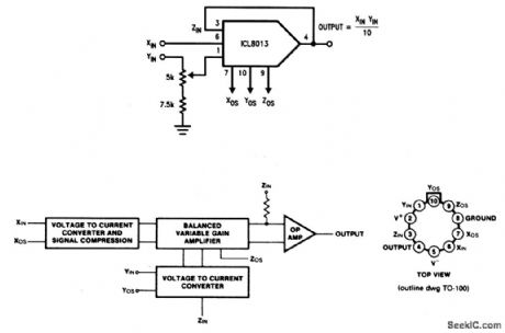
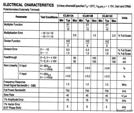
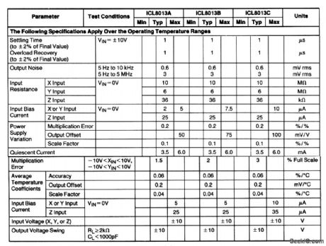
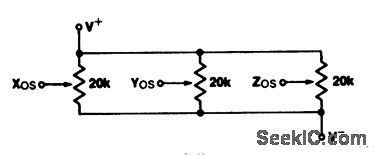
This circuit shows an ICL8013 four-quadrant multiplier connected as a basic multiplier. Figure 3-15B shows the pin connections and functional diagram. Figure 3-15C shows the electrical characteristics. Figure 3-15D shows the connections for trimming offset and feedthrough. Use the following trim procedure.
1. Set XIN= YIN= 0 V, and adjust Z0S for zero output.2. Apply a±10-V low-frequency (below 100 Hz) sweep (sine or triangle) to YINwith XIN 0 V, and adjust X0S for minimum output (chapter 5 contains several sweep-generator circuits).3. Apply the sweep signal of step 2 to XIN with YIN= 0 V, and adjust Y0s for minimum output.4. Readjust Z0s, as in step 1, if necessary.5. With XIN =10.0 Vdc, and the sweep signal of step 2 applied to YIN, adjust the gain potentiometer until the output equals YIN. This can be done with a differential scope plug-in (A + B) by inverting one signal and adjusting the gain control for (output - YIN)=0. (View)
View full Circuit Diagram | Comments | Reading(797)
OTA_four_quadrant_multiplier
Published:2009/7/24 23:51:00 Author:Jessie
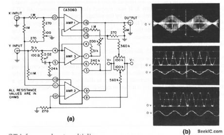
This circuit uses all three sections of an OTA to form a four-quadrant multiplier. To adjust the circuit, remove all signals from the X and Y inputs, connect pin 10 to pin 8 (to disable amp 2), and set the Amp 1 offset to zero with the 100-kΩ potentiometer (adjust the pot until the output is zero). Disconnect pin 10 from pin 8, and connect pin 15 to pin 8 (to disable amp 1), and set the Amp 2 offset to zero with the corresponding 100-kΩ pot (adjust the pot until the output is zero). Disconnect pin 15 from pin 8. Apply equal ac signals to both the X and Y inputs. Adjust the 100-Ω and 200-kΩ pots for symmetrical output signals. Figure 11-2B shows the output waveform with the multiplier adjusted. The voltage waveform in Fig. 11-2Ba shows suppressed-carrier modulation of the 1-kHz carrier with a triangle wave. Figures 11-2Bb and 11-2Bc, respectively, show the squaring of a triangular wave and a sine wave. Notice that in both cases, the output are always positive and return to zero after each cycle. (View)
View full Circuit Diagram | Comments | Reading(2590)
Reset_timer_astable_operation
Published:2009/7/24 23:48:00 Author:Jessie
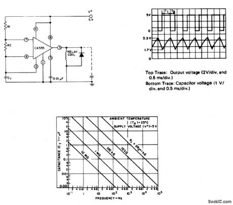
This circuit shows how a CA555 timer can be connected for astable (free-running) operation. Figure 3-13B shows typical waveforms. Figure 3-14C shows free-running frequency versus Rc for various values of R1 + R2 and CT.Notice that the total period is a function of both R1 and R2 as shown by T= 0.693 (R1 +R2)T C and t2= 0.6983 (R2)CT The duty cycle is t2/(t1+t2)= R2/(R1+ 2R2). (View)
View full Circuit Diagram | Comments | Reading(680)
Schmitt trigger circuit and its trigger characteristics
Published:2011/8/1 2:39:00 Author:Ecco | Keyword: Schmitt , trigger circuit, characteristics
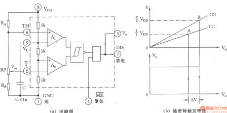
The chart shows a Schmitt trigger with adjustable threshold voltage composed of 555 time base circuit and RA, RB, RP. It could be viewed as the Schmitt trigger circuit driven by comparator. The output has two ports: One is the rectangular pulse output by pin 3; the other one is the discharging wave (external capacitor) output by pin 7 of the discharging end.
(View)
View full Circuit Diagram | Comments | Reading(1491)
Norton_peak_detector
Published:2009/7/24 23:48:00 Author:Jessie
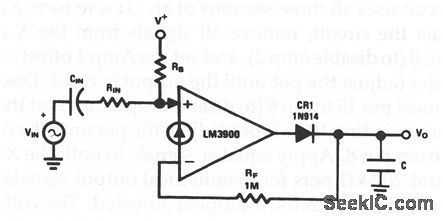
In this circuit, the Norton is used to rapidly charge capacitor C to peak value of Vin. The voltage drop across CR1 is placed within the feedback loop to prevent voltage losses and temperature drifts in the output voltage. The feedback resistor (RF) is kept small (1 MΩ) so that the 30-nA base current of the Norton will cause only a +30-mV error in output voltage VO. Feedback resistor RF is con-stantly loading C, in addition the current drawn by the circuitry which samples VO. Bias resistor RB allows a minimum dc voltage to exist across C. Overall circuit gain is set by the value of RIN in relation to RF. (View)
View full Circuit Diagram | Comments | Reading(720)
Electronic hypnotic device 2
Published:2011/8/1 2:25:00 Author:Ecco | Keyword: Electronic , hypnotic device
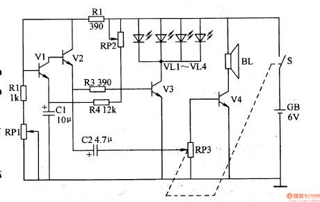
The electronic hypnotic device decribed in the example cangenerate simulated sound of dripping water, but also issue a low-frequency synchronized flashing signal, it is easy to reduce the tension, and the users will quickly go to sleep by listening to dripping water sound or watching flashing LED watch (LED), . The device can also be used as a stutter appliance.
The working principle.
The electronic circuit is composed of the oscillator circuit and LED drive circuit and audio circuit, andit is shownas Figure 9-139.
Oscillator circuit consists of transistors Vl, V2 and related peripheral components. LED driver circuit consists of the transistor V3 and LED VLl-VL4. Audio circuit consists of transistor V4, coupling capacitor C2, and speaker BL, volume potentiometer RW. Turning the power switch S, the oscillator circuit oscillates, the emitter of V2 outputs oscillation signal. The oscillation signal is amplified by V3 to drive VLl-VL4 shining; another path is amplified by V4 to drive speaker BL toissue the sound of dripping water. Adjusting potentiometer RP2, RPl can change the oscillator frequency, thus changing the speed of sound dripping and LED flash frequency.
(View)
View full Circuit Diagram | Comments | Reading(1135)
Reset_timer_monostable_operation
Published:2009/7/24 23:45:00 Author:Jessie
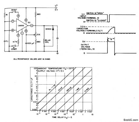
This circuit shows how a CA555 timer can be connected for monostable operation. Figure 3-13B shows typical waveforms. Figure 3-13C shows time delay versus RC for various values of R1 and C1. (View)
View full Circuit Diagram | Comments | Reading(669)
Power_op_amp_with_remote_sensing
Published:2009/7/24 23:45:00 Author:Jessie
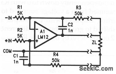
This circuit shows an LM12 (Fig. 10-46) connected as a differential-input amplifier with dc feedback from a remotely sensed load. The ac feedback is directly from the op-amp output and the signal common at the sending end. There is no feedback from the load at high frequencies. The optimum capacitance for C1/C2 depends on the cable delay. Note that the common and LM12 output cables must be capable of carrying a typical 10A, whereas the feedback-sensing cables can be small. For a single-ended input, strap the unused input terminal to common. (View)
View full Circuit Diagram | Comments | Reading(914)
Power_op_amp_voltage_regulator_with_overvoltage_protection
Published:2009/7/24 23:44:00 Author:Jessie
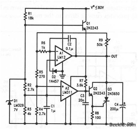
This circuit shows an LM12 (Fig, 10-46) connected with other components to form a positive regulator. The output is 4-70V, set by R9. Should the LM12 not be able to control an overvoltage condition, the SCR Q3 will crowbar the output. (View)
View full Circuit Diagram | Comments | Reading(745)
5_V_from_two_to_three_cells_low_cost_micronpower
Published:2009/7/24 23:26:00 Author:Jessie
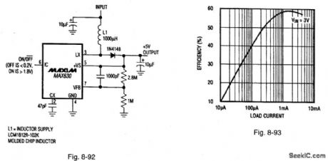
Figure 8-92 shovgs a MAX630 connected to provide a low-cost, micropower 5-V output, with a 1.6-V to 5-V input range. Figure 8-93 shows the efficiency curve. The quiescent current is 160 μA, with a start-up of 2 V, a maximum load current of 5 mA, and a shutdown current of 1 μA. This current is most useful in micropower applications where cost, not efficiency, is the main concern. (Efficiency can be improved by substituting a Schottky rectifier for the 1N4148, and a low-resistance inductor for L1, at the expense of higher cost.) The circuit is boot-strapped (+Vs connected to the +5-V output). In those applications where minimum start-up voltage is essential, connect the +Vs pin directly to the input. Unfortunately, removing the boot-strap connection is done at the expense of low-voltage load-current capability. MAXIM BATTERY MANAGEMENT CIRCUIT COLLECTION, 1994, P. 14. (View)
View full Circuit Diagram | Comments | Reading(648)
TRANSFORMERLESS_BALANCED_INPUT_MI_CROPHONE_PREAMP
Published:2009/6/29 2:26:00 Author:May
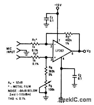
Uses FET-input opanlp to amplify differential signals while rejecting common-mode signals. Gain is set at 52 dB by ratio of R3 to R1. Input resistors R1 and R2 are made large compared to source impedance while being kept as small as possible, for optimum balance between input loading effects and low noise. Good compromise value is 10 times source impedance for R1 + R2.- Audio Handbook, National Semiconductor, Santa Clara, CA, 1977, p 2-37-2-40. (View)
View full Circuit Diagram | Comments | Reading(900)
SEQUENTIAL_TIMING
Published:2009/6/29 2:26:00 Author:May

By utilizing both halves of the dual timer it is possible to obtain sequential timing. By con-necting the output of the first half to the input of the second half via a.001 μF coupling capacitor, sequential timing may be obtained. Delay h is determined by the first half and t2 by the second half delay. The first half of the timer is started by momentarily connecting pin 6 to ground. When it is timed out (determined by 1.1R1C1) the second half begins. Its time dura-tion is determined by 1.1R2C2. (View)
View full Circuit Diagram | Comments | Reading(693)
Power_op_amp_voltage_current_converter
Published:2009/7/24 23:25:00 Author:Jessie

As shown by the equation, this LM12 (Fig. 10-46) circuit provides an output current proportional to input voltage. This circuit requires precise resistor matching, and/or trimming by R3, to get high output resistance. Any inductance in R6 will reduce bandwidth. (View)
View full Circuit Diagram | Comments | Reading(874)
| Pages:1250/2234 At 2012411242124312441245124612471248124912501251125212531254125512561257125812591260Under 20 |
Circuit Categories
power supply circuit
Amplifier Circuit
Basic Circuit
LED and Light Circuit
Sensor Circuit
Signal Processing
Electrical Equipment Circuit
Control Circuit
Remote Control Circuit
A/D-D/A Converter Circuit
Audio Circuit
Measuring and Test Circuit
Communication Circuit
Computer-Related Circuit
555 Circuit
Automotive Circuit
Repairing Circuit