
Circuit Diagram
Index 1244
3-1 Pulse Frequency Dividing Circuit
Published:2011/7/21 0:39:00 Author:Joyce | Keyword: 3-1, Pulse Frequency , Dividing

In digital circuits, sometimes a frequency dividing circuit is needed to subtract a few pluses from an input pulse. Appropriate composition of CD4013 and feedback gate can make almost any circuit combination of pulse subtraction. As shown in the figure is a 3-1 pulse frequency dividing circuit composed of CD4013.
(View)
View full Circuit Diagram | Comments | Reading(692)
Bilateral_current_source
Published:2009/7/24 22:12:00 Author:Jessie
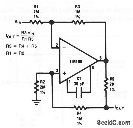
This circuit is similar to that of Fig. 10-25, except that the adjustment circuit is omitted (and the circuit is simplified). (View)
View full Circuit Diagram | Comments | Reading(0)
Window_detector
Published:2009/7/24 22:11:00 Author:Jessie
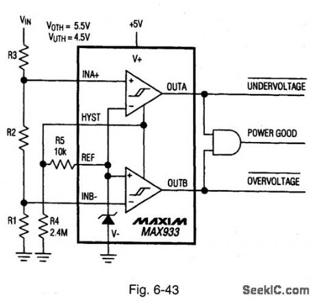
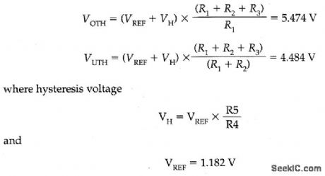
Figure 6-43 shows a MAX933 comparator connected as a window detector (see Fig. 6-42 for pin connections). For the voltage thresholds shown (5.5 V upper and 4.5 V lower), use 249 kΩ, 61.9 kΩ, and 1 MΩ for R1, R2, and R3 respectively. Verify these resistor values using the following equations:Other threshold values can be selected by choice of the R1, R2, and R3, values, using the same equations. MAXIM NEW RELEASES DATA BOOL, 1995, P. 3-57. (View)
View full Circuit Diagram | Comments | Reading(2)
High-precision 50Hz Time Base Signal Source Circuit
Published:2011/7/21 1:14:00 Author:Joyce | Keyword: High-precision , 50Hz , Time Base , Signal Source
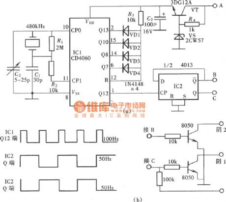
In some early digital electronic clocks supplied by ac, 50 Hz ac power supply is used as time base signal for second after frequency division because of circuit structure. Since small deviation is inevitable for the frequency of the ac power supply, major deviation from actual time will be created after years later. In order to eliminate the deviation, some amateurs have made various kinds of high precision 50 Hz time base circuits, among which the circuit composed of CD4060 is most commonly used. It is as shown in the figure. (View)
View full Circuit Diagram | Comments | Reading(2714)
NICKEL_CADMIUM_CELL_CHARGER
Published:2009/6/29 20:43:00 Author:May
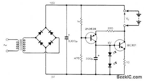
Charges four size D cells in series at constant current, with automatic voltage limiting. BC301 transistor acts as current source, with base voltage stabilized at about 3 V by two LEDs that also serve to indicate charge condition. Other transistor provides voltage limiting when voltage across cekks approaches that of 1k branch of voltage divider. Values shown give 260-mA charge initially, dropping to 200 mA when VC reaches 5V and decreasing almost to 0 when VCreaches 6.5 V.-N.H. Sabah, Battery Charger, Wireless World, Nov. 1975, p 520. (View)
View full Circuit Diagram | Comments | Reading(1043)
TUNABLE_NOTCH_FILTER_TO_SUPPRESS_HUM
Published:2009/6/29 4:41:00 Author:May
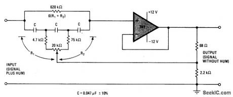
Circuit Notes
This narrow-stop-band filter can be tuned by the pot to place the notch at any frequency from 45 to 90 Hz. It attenuates power-line hum or other unwanted signals by at least 30 dB.Because the circuit uses wide-tolerance parts, it is inexpensive to build. (View)
View full Circuit Diagram | Comments | Reading(777)
Automatic_power_off_switch
Published:2009/7/24 22:09:00 Author:Jessie
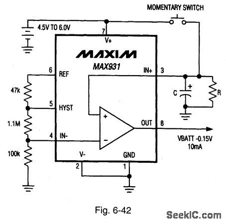
Figure 6-42 shows a MAX931 comparator connected as a timed, automatic power-off circuit for a 40-mA supply. The comparator output is the supply output. With a 10-mA load, the circuit provides a voltage of (VBATT-0.12 V), but it draws only 3.5 μA of quiescent current. Using the values shown, the three-resistor voltage divider programs the maximum ±50 mV of hysteresis and sets the IN- voltage at 100 mV. This gives an IN+ trip threshold of about 50 mV for the IN+ falling. The RC time constant determines the maximum power-on time of the OUT pin (8) before power-down occurs. This period (in seconds) can be approximated by: R×C×4.6. For example: 2 M×10 μF×4.6=92 (seconds). MAXIM NEW RELEASES DATA BOOK, 1995, P, 3-57. (View)
View full Circuit Diagram | Comments | Reading(1049)
HARTLEY_OSCILLATOR
Published:2009/6/29 4:41:00 Author:May
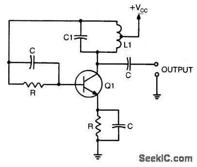
Resonant frequency is 1/2 π √LIC1. (View)
View full Circuit Diagram | Comments | Reading(0)
FOURTH_ORDER_HIGH_PASS_BUTTERWORTH_FILTER
Published:2009/6/29 4:38:00 Author:May
View full Circuit Diagram | Comments | Reading(0)
2_MHz_OSCILLATOR_
Published:2009/6/29 4:37:00 Author:May
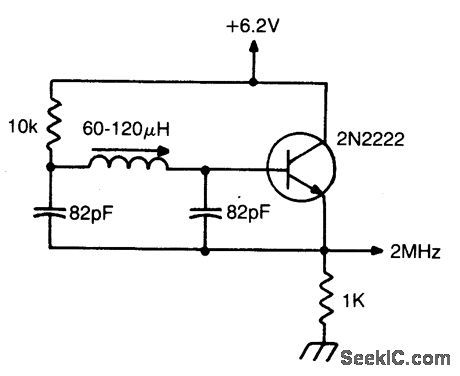
Miller 9055 miniature slugtuned coil;allresistors 1/4W 5%;all caps mln.25 V ceramic. (View)
View full Circuit Diagram | Comments | Reading(864)
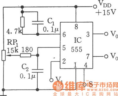
RS Trigger Operating Principle Circuit
Published:2011/7/23 1:15:00 Author:Joyce | Keyword: RS , Trigger , Operating Principle
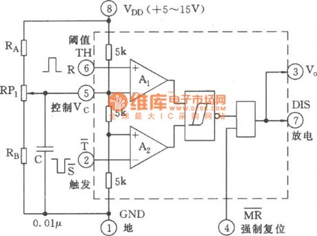
As shown in the figure is a circuit in which 555 works as a RS trigger. If the control voltage on the controlling end feet 5 is removed, there will be no need to connect any external component with 555, but add negative and positive control pulse on feet 2 and 6 respectively to constitute a RS trigger circuit. End R is the reset control input end feet 6, which is also called threshold end (TH);end S is the set control input feet 2, which is also called set trigger end T. The output end (feet 3) within the chip is actually push-pull output, whose low level output is only about 0.3 V and whose high level is close to VDD, so it has a very strong load capacity (View)
View full Circuit Diagram | Comments | Reading(1090)
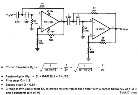
10_kHz_SALLEN_KEY_LOW_PASS_FILTER
Published:2009/6/29 4:36:00 Author:May
View full Circuit Diagram | Comments | Reading(702)
Schmidt Trigger Circuit and its Trigger Characteristics Circuit
Published:2011/7/21 21:44:00 Author:Joyce | Keyword: Schmidt , Trigger , Characteristics
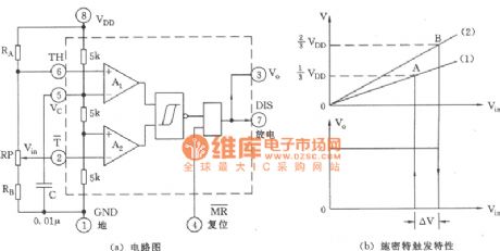
As shown in the figure is a Schmitt trigger composed of time base circuit 555 and a few other components ( RA, RB, RP ). Its threshold voltage is adjustable. It can be seen as being triggered by the comparator. It has two output ends: one is rectangular pulse output by feet 3; the other is discharging waveform (circumscribed capacitor) output by the discharge end (DSC) feet7. (View)
View full Circuit Diagram | Comments | Reading(890)
10_MHz_OSCILLATOR
Published:2009/6/29 4:36:00 Author:May
View full Circuit Diagram | Comments | Reading(774)
Changeable Threshold Level Trigger Circuit
Published:2011/7/21 21:54:00 Author:Joyce | Keyword: Changeable , Threshold , Level, Trigger
As shown in the figure, with the setting characteristics of reset end feet 4 and trigger end feet 2 of 555, it can compose a RS trigger. Feet 5 is connected with the pressure dividing point 2/3 VDD of the resistance within the substrate. Adding an adjustable control voltage on feet 5 would change the threshold level and trigger level to compose a changeable threshold level Schmidt trigger. C1, C2 are high frequency filter capacitances used to decoupling. (View)
View full Circuit Diagram | Comments | Reading(632)
DIGITALLY_TUNED_LOW_POWER_ACTIVE_FILTER
Published:2009/6/29 4:35:00 Author:May
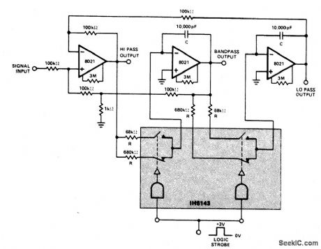
Circuit NotesConstant gain, constant Q, variable frequency filter which provides simultaneous low-pass, bandpass, and high-pass outputs.With the component values shown, center frequency will be 235 Hz and 23.5 Hz for high and low logic inputs respectively, Q=100, and gain=100.
fn=center frequency =1/2πRC (View)
View full Circuit Diagram | Comments | Reading(782)
400_MHz_OSCILLATOR_
Published:2009/6/29 4:35:00 Author:May
View full Circuit Diagram | Comments | Reading(823)
Biostable Control Circuit
Published:2011/7/21 8:58:00 Author:Joyce | Keyword: Biostable , Control
Bistable mode of 555 is applied less commonly compared with monostable mode and nonstable mode. Bistable mode means the circuit it forms will be triggered by pressing R-S. As shown in the figure is micro-motor’s forward/reserve control diagram working under biostable mode. (View)
View full Circuit Diagram | Comments | Reading(573)
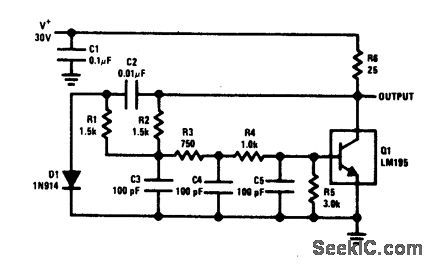
LOW_DISTORTION_OSCILLATOR
Published:2009/6/29 4:34:00 Author:May
The 2N5485 JFET is capable of oscillating in a circuit where harmonic distortion is very low. The JFET local oscillator is excellent when a low harmonic content is required for a good mixer circuit. (View)
View full Circuit Diagram | Comments | Reading(0)
NISSAN new Teana audio (with navigation system) circuit (d)
Published:2011/7/26 4:58:00 Author:John | Keyword: navigation system, new Teana audio
NISSAN new Teana audio (with navigation system) circuit(d)is shown.
(View)
View full Circuit Diagram | Comments | Reading(847)
| Pages:1244/2234 At 2012411242124312441245124612471248124912501251125212531254125512561257125812591260Under 20 |
Circuit Categories
power supply circuit
Amplifier Circuit
Basic Circuit
LED and Light Circuit
Sensor Circuit
Signal Processing
Electrical Equipment Circuit
Control Circuit
Remote Control Circuit
A/D-D/A Converter Circuit
Audio Circuit
Measuring and Test Circuit
Communication Circuit
Computer-Related Circuit
555 Circuit
Automotive Circuit
Repairing Circuit