
Circuit Diagram
Index 1255
ELECTROSTATIC_HEADPHONES
Published:2009/6/29 1:54:00 Author:May
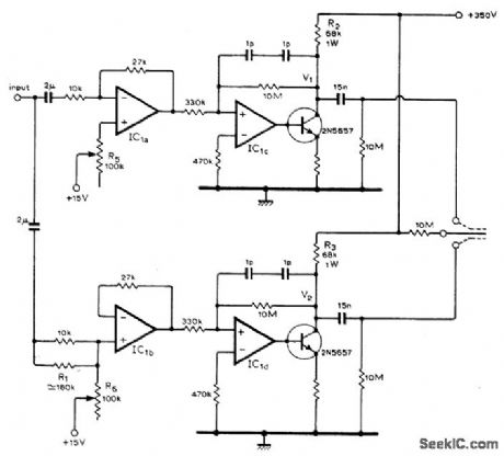
Uses LM3900N four-opamp IC and two transistors to step up headphone output signal of AF power amplifier sufficiently to drive pair of electrostatic headphones without introducing excessive distortion. Total harmonic distortion at 1 kHz is 1% at 300-V peak-to-peak output, and dropsto 0.1% at 50-V output.-N. Pollock, Elec-trostatic Headphone Amplifier, Wireless World, July 1976, p 35. (View)
View full Circuit Diagram | Comments | Reading(2897)
_5_V_from_a_charge_pump_micropower
Published:2009/7/25 4:19:00 Author:Jessie
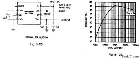
Figure 8-124 shows a MAX1044 charge pump connected to provide -5 V atmicropower. Figure 8-125 shows the efficiency curve.The input voltage range is 1.5 V to 10 V output impedance is 65 Ω quiescent current is 50 μA( VIN =5 V),maximum load current is 10 mA (VIN = 4.75 V) and shutdown current is 1.5 μA.This circuit is a scaled-down verslon of the Fig.8-122,The MAX1044 is basicallyidentical to the MAX660 except for a somew,hat higher input-voltage range, a 10-times-reduced output-current, and lower cost. The fixed-frequency oscillator range is 8 to 65 kHz.MAXIM BATTERY MANAGEMENT CIRCUIT COLLECTION, 1994, P. 61.
(View)
View full Circuit Diagram | Comments | Reading(756)
IC_precision_oscillator_with_a_split_supply
Published:2009/7/25 4:17:00 Author:Jessie
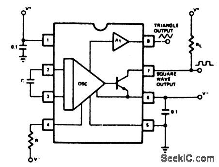
This circuit is similar to that of Fig. 5-44, except that the circuit requires a split supply greater than 7V, and simplifies the bias power connections at pins 5 and 6. Note that the triangle output has a +0.6-V offset when this circuit is used. (View)
View full Circuit Diagram | Comments | Reading(622)
BALANCED_OUTPUT_WITH_OPAMPS
Published:2009/6/29 1:53:00 Author:May
Low-cost amplifier provides lowimpedance balanced output from unbalanced signal output of preamp. Response is flat from 10 to 20,000 Hz, and distortion less than 0.1% at 800 Hz into 600-ohm load. Gain is 20 dB. Other opamps, such as LM307 or 747 (dual 741) can also be used.K. D. James, Balanced Output Amplifier, Wireless World, Doc. 1975, p 576. (View)
View full Circuit Diagram | Comments | Reading(3230)
IC_precision_oscillator_with_a_single_supply
Published:2009/7/25 4:16:00 Author:Jessie
This circuit is similar to that of Fig. 5-44, except that a single supply isused. (View)
View full Circuit Diagram | Comments | Reading(1537)
ERROR_TAKEOFF_REDUCES_DISTORTION
Published:2009/6/29 1:52:00 Author:May
Nonlinear distortion is reduced in singleended amplifier by producing voltage proportional to distortion and amplifying this error voltage in such a way thatit can be used to reduce distortion at output. Circuit uses 741 opamps and MJ4000 power Darlington transistors. Technique overcomes basic Iimitation of negative feedback wherein feedback loop gain decreases as frequency increases. Artide also gives variation of circuit more suitable for power amplifier, and describes circuit operation in detail.-A. M. Sandman, Reducing Amplifier Distortion, Wireless World, Oct. n974, p 367-371. (View)
View full Circuit Diagram | Comments | Reading(764)
Low_distortion_sine_wave_oscillator_1
Published:2009/7/25 3:31:00 Author:Jessie
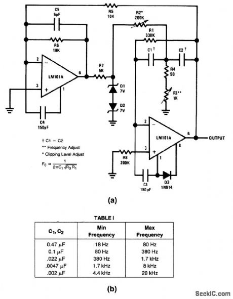
This circuit provides sine-wave outputs at frequencies shown in Fig.5-14B with low distortion (between 0.2% and 0.4% for 20% clipping, as set by R2).The frequency is set by R1, R3, and C1 as shown. (View)
View full Circuit Diagram | Comments | Reading(875)
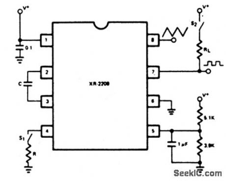
TEMPERATURE_TO_FREQUENCY_CONVERTER
Published:2009/6/29 1:52:00 Author:May
The circuit exploits the fact that when fed from a constant current source, the forward voltage of a silicon diode varies with temperature in a reasonably linear way. Diode D1 and resistor R2 form a potential divider fed from the constant current source. As the temperature rises, the forward voltage of D1 falls tending to turn Q1 off. The output voltage from Q1 will thus rise, and this is used as the control voltage for the CMOS VCO. With the values shown, the device gave an increase ofjust under 3 Hz/℃ (between 0 ℃ and 60 ℃) giving a frequency of 470 Hz at 0 ℃. (View)
View full Circuit Diagram | Comments | Reading(0)
15W audio power amplifier circuit diagram composed of OPA604
Published:2011/8/1 3:03:00 Author:Ecco | Keyword: 15W , audio power amplifier
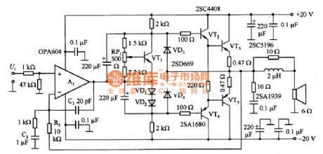
Figure 1 is l5W audio power amplifier circuit constituted by the OPA604. OPA604 has FET-input with the working voltage in ± 25V, and the conversion rate in 25V/μs, and GB is the 2OMHz excellent high-frequency op amp, which is used as the pre-amplifier to get low-level distortion. RP1 is used to adjust the load current of power transistor in 35mA; VD3 and VD4 are used to limit output current in short circuit, and when the circuit works normally, they are in the cut-off state.
(View)
View full Circuit Diagram | Comments | Reading(4635)
Low_distortion_sine_wave_oscillator
Published:2009/7/25 3:12:00 Author:Jessie
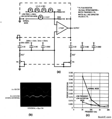
This circuit uses the positive temperature coefficient of lamp filaments in a modem adaptation of a classic oscillator circuit. A variable Wien bridge provides frequency tuning form 20 Hz to 20 kHz. Figure 5-1B shows the oscillator waveforms, while oscillator distortion versus is plotted in Fig. 5-1C. (View)
View full Circuit Diagram | Comments | Reading(2515)
VOLTAGE_CONTROLLED_HYSTERESIS
Published:2009/6/29 1:52:00 Author:May
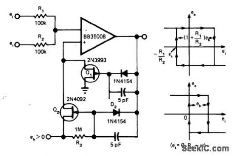
Pre-cise, independent control of comparator trip point and hysteresis is achieved by switching hysteresis control signal eh to comparator input with Q1 and Q2 when opamp changes state. Circuit avoids hysteresis feedback error while achieving inherent 0.01% trip-point accu racy of comparator. Control voltage et determines first trip point. When opamp output is negative, Q2 is held off and Q1 is on for connecting noninverting input to ground. Output switching oc curs when input signal ei drives input of inverting amplifier to zero.—J. Graeme, Comparator Has Precise, Voltage-Controlled Hysteresis, EDN Magazine, Aug. 20, 1975, p 78 and 80. (View)
View full Circuit Diagram | Comments | Reading(921)
VOLTAGE_COMPARATOR
Published:2009/6/29 1:50:00 Author:May
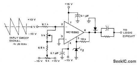
Motorola MC1539 opamp provides excellent temperature characteristics and very high slewing rate for comparator applications. Zener connected to pin 5 Limits positive-going waveform at output to about 2 V below zener voltage. Silicon diode connected to output limits negative excursion of output to give protection for logic circuit being driven. Parallel RC network in output provides impedance matching and minimizes output current overload problems.—E. Renschler, The MC1539 Operational Amplifier and Its Applications, Motorola, Phoenix, AZ, 1974, AN-439, p 18. (View)
View full Circuit Diagram | Comments | Reading(1870)
RS_232_power_supply
Published:2009/7/25 3:10:00 Author:Jessie
This circuit operates with inputs as low as 4.2 V, and delivers an output of±12 V at ±40 mA with an efficiency of better than 70%. Load regulation is ±1.25% (from 10% to 100% of full load) and line regulation is ±0.08%, with less than 40-mV pp ripple. (View)
View full Circuit Diagram | Comments | Reading(829)
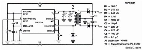
Step_up__30_V_to_100_V_at_100_mA_flyback_converter
Published:2009/7/25 1:42:00 Author:Jessie
This circuit converts 30-V to 100-V(adjustable)output. (View)
View full Circuit Diagram | Comments | Reading(778)
CASCODE_AMPLIFIER
Published:2009/6/29 1:50:00 Author:May
Uses two sections of RCA CA3028A IC near IC(U1A is not used) Provides power gain of about 40 dB,Unmarked resistors are on IC,-D DeMaw,Understanding Linear ICs QST,Feb,1977、p 19-23 (View)
View full Circuit Diagram | Comments | Reading(1595)
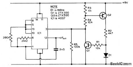
Norton_true_noninverting_integrator
Published:2009/7/25 1:41:00 Author:Jessie
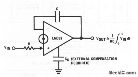
This circuit shows a Norton used as a noninverting integrator, where the output changes in accordance with a constant times that the time integral of the input. This classic op-amp circuit was originally developed to perform the mathematical operation of integration in analog computers. However, most op-amp integrators are inverting where VIN is applied to the (-) input. Pin numbers for the Norton IC are shown in Fig. 11-15. (View)
View full Circuit Diagram | Comments | Reading(1833)
HIGH_OUTPUT_CUfIRENT
Published:2009/6/29 1:49:00 Author:May
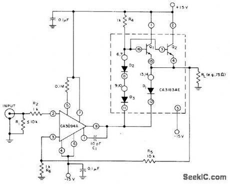
Uses CA3094A programmable opamp as driver stage for two parallel-connected transistors of CA3183AE arrayto develop 100-mA average AF current(peaks up to 300mA)through 75-ohm load,Diode-connected transistors D1-D3 in array provide temperature compensation for output tranperature- Circuit ldeas for RCA Linear ICs、″RCA solid State Division Somerville,NJ,1977、p11 (View)
View full Circuit Diagram | Comments | Reading(794)
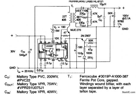
Step_up_step_down_6__to_22__to_12_Vdc_converter
Published:2009/7/25 1:41:00 Author:Jessie

This circuit converts 6 V to 22 V (through operation of a switching regulator) and then reduces the 22 V to a fixed 12 V (through operation of an LAS1612 linear regulator). (View)
View full Circuit Diagram | Comments | Reading(657)
μpCl350C monolithic playback IC diagram
Published:2011/8/1 3:03:00 Author:Ecco | Keyword: monolithic playback IC
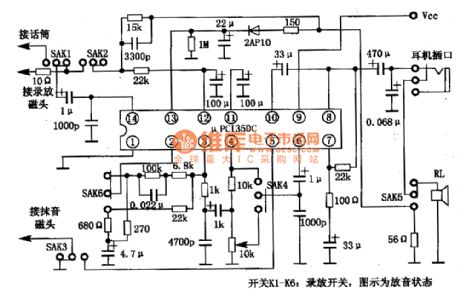
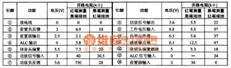
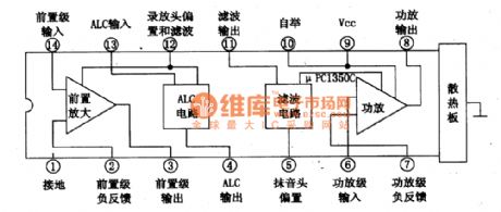
μPCl350C monolithic playback IC produced by Japan NEC (electrical) is widely used in a variety of small recorders, stereo systems etc. 1.μPCl350C block diagram and pin functions μPCl350C manifold is a complete recording circuit, which is composed of the preamplifier, automatic level control (ALC) and the power amplifier circuit. The manifold block diagram is shown in Figure 1-1. The IC uses 14-pin dual in-line package, and the integrated circuit pin functions and data are listed in Table 19-3.
(View)
View full Circuit Diagram | Comments | Reading(779)
0°F_50°F_THERMOMETER
Published:2009/6/29 1:49:00 Author:May
View full Circuit Diagram | Comments | Reading(851)
| Pages:1255/2234 At 2012411242124312441245124612471248124912501251125212531254125512561257125812591260Under 20 |
Circuit Categories
power supply circuit
Amplifier Circuit
Basic Circuit
LED and Light Circuit
Sensor Circuit
Signal Processing
Electrical Equipment Circuit
Control Circuit
Remote Control Circuit
A/D-D/A Converter Circuit
Audio Circuit
Measuring and Test Circuit
Communication Circuit
Computer-Related Circuit
555 Circuit
Automotive Circuit
Repairing Circuit