
Circuit Diagram
Index 1245
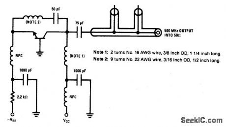
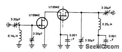
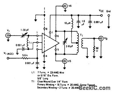
500_MHz_OSCILLATOR
Published:2009/6/29 4:33:00 Author:May
View full Circuit Diagram | Comments | Reading(739)
Silicon Controlled Trigger Circuit
Published:2011/7/21 9:08:00 Author:Joyce | Keyword: Silicon Controlled, Trigger
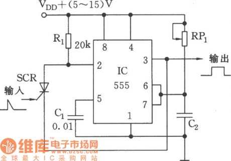
As shown in the figure, 555, R1, RP1, C2 and some other components constitute the trigger delay circuit. Commonly, 555 is in the state of reset , and feet 3 displays a low level since R1 is connected with VDD; When triggered signals come in , SCR will break over ,feet 2 will have a low level signal which will turn 555 to output a high level. The temporary stable width is: τ = 1.1 RP1C2 . After triggering, SCR will shut off. This circuit can lower the requirement of triggering pulse. If CMOS type 555 (or 556) is used, the triggering current can also be reduced. (View)
View full Circuit Diagram | Comments | Reading(752)
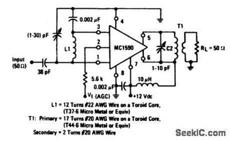
FIVE_POLE_ACTIVE_FILTER
Published:2009/6/29 4:30:00 Author:May
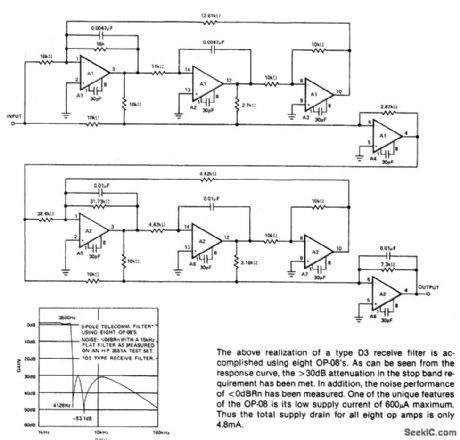
The above realization of a type D3 receive filter is accompished using eight OP-08's. As can be seen from 1he response curve the >30dB attenuation in the stop band re-qu jrement has been met. In addition, thenoise performance of <0dBHn has been measured. One of the unique features of the OP-08 is ils low supply current of 600μA maximum Thus the total supply dralrl for all eight op amps is only 4.8mA. (View)
View full Circuit Diagram | Comments | Reading(707)
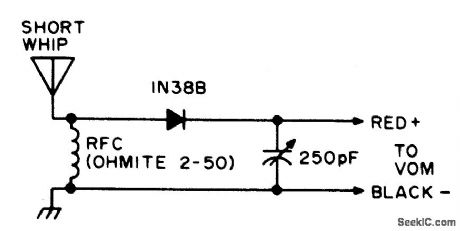
VOM_FIELD_STRENGTH_METER
Published:2009/6/29 4:26:00 Author:May
View full Circuit Diagram | Comments | Reading(716)
450_MHz_COMMON_SOURCE_AMPLIFIER
Published:2009/6/29 4:26:00 Author:May
View full Circuit Diagram | Comments | Reading(678)
High Frequency Thyristor Trigger Circuit
Published:2011/7/21 9:16:00 Author:Joyce | Keyword: High Frequency , Thyristor , Trigger
As shown in the figure, 555 ,RP1, R2, C1 constitute the astable multivibrator.The oscillation frequency and duty ratio can be altered by adjusting RP1. The output pulse will trigger the flip-flop composed of VT1 and VT2. V01, V02 can trigger two thyristors alternatively .
(View)
View full Circuit Diagram | Comments | Reading(1537)
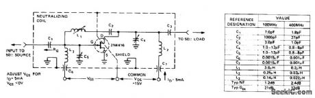
200_MHz_NEUTRALIZED_COMMON_SOURCE_AMPLIFIER
Published:2009/6/29 4:26:00 Author:May
View full Circuit Diagram | Comments | Reading(575)
TUNED_FIELD_STRENGTH_METER
Published:2009/6/29 4:25:00 Author:May
Circuit NotesResonant combination of L1 and C1 selected to cover frequencies desired. (View)
View full Circuit Diagram | Comments | Reading(737)
80_MHz_CASCODE_AMPLIFIER
Published:2009/6/29 4:25:00 Author:May
View full Circuit Diagram | Comments | Reading(1070)
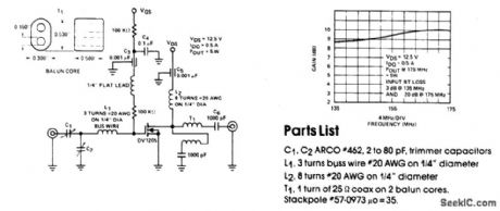
TWO_METER_AMPLIFIER5_W_OUTPUT
Published:2009/6/29 4:24:00 Author:May
View full Circuit Diagram | Comments | Reading(621)
UNTUNED_FIELD_STRENGTH_METER
Published:2009/6/29 4:24:00 Author:May
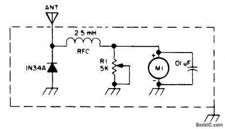
Circuit Notes
Sensitivity is controlled by R1 and sen-sitivity of Meter M1. (View)
View full Circuit Diagram | Comments | Reading(688)
30_MHz_AMPLIFIER_POWER_GAIN=50_dBBW≈10_MHz
Published:2009/6/29 4:23:00 Author:May
View full Circuit Diagram | Comments | Reading(482)
60_MHz_AMPLIFIER
Published:2009/6/29 4:23:00 Author:May
View full Circuit Diagram | Comments | Reading(612)
TRANSISTORIZED_Q_MULTIPLIER_FOR_USE_WITH_IFS_IN_THE_1400_kHz_RANGE
Published:2009/6/29 4:21:00 Author:May
View full Circuit Diagram | Comments | Reading(838)
UHF_AMPLIFIER_WITH_INVERTING_GAIN_OF_2_AND_LAG_LEAD_COMPENSATIONGAIN_BANDWIDTH_PRODUCT_350_MHz
Published:2009/6/29 4:20:00 Author:May
View full Circuit Diagram | Comments | Reading(826)
ULTRA_HIGH_FREQUENCY_AMPLIFIER
Published:2009/6/29 4:19:00 Author:May
View full Circuit Diagram | Comments | Reading(717)
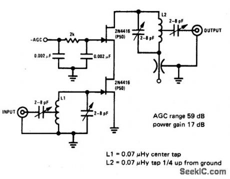
100_MHz_AND_400_MHz_NEUTRALIZED_COMMON_SOURCE_AMPLIFIER
Published:2009/6/29 4:18:00 Author:May
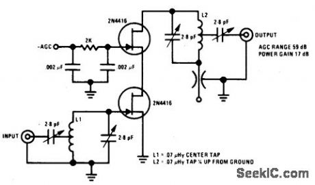
View full Circuit Diagram | Comments | Reading(648)
135_175_MHz_AMPLIFIER
Published:2009/6/29 4:16:00 Author:May
View full Circuit Diagram | Comments | Reading(636)
200_MHz_CASCODE_AMPLIFIER
Published:2009/6/29 4:15:00 Author:May
This 200 MHz JFET cascode circuit features low cross-modulation, large signal handling ability, no neutralization, and AGO controlled by biasing the upper cascade JFET. The only special requirement of this circuit is that bss of the upper unit must be greater than that of the lower unit. (View)
View full Circuit Diagram | Comments | Reading(1162)
800Hz Signal Generator Circuit
Published:2011/7/20 23:42:00 Author:Joyce | Keyword: 800Hz , Signal Generator
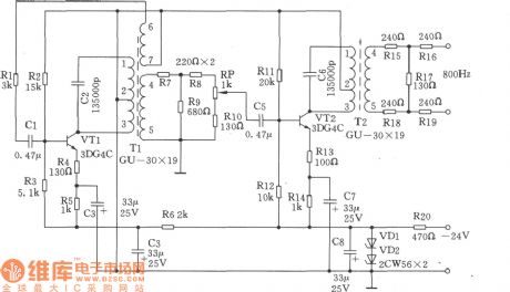
The oscillation stage of this 800 Hz signal generator is a transformer coupling LC oscillating circuit, which is simple and has a stable frequency. Control amplifier is used as buffer amplifier to reduce distortion, and potentiometer can be used to adjust the output level. 1. The technical index (1)operating frequency : 800 Hz ; (2) frequency stability:≤士 20 Hz ; (3) output level: 0 dB / 600 Ω. 2. Working principle is as shown in the figure. The 800 Hz signal generator is composed of LC oscillation stage and buffer amplifier stage. Oscillation stage: The tuned transformer T1 is used as LC oscillation tank circuit and output transformer, and C2 is a tuned capacitor. (View)
View full Circuit Diagram | Comments | Reading(838)
| Pages:1245/2234 At 2012411242124312441245124612471248124912501251125212531254125512561257125812591260Under 20 |
Circuit Categories
power supply circuit
Amplifier Circuit
Basic Circuit
LED and Light Circuit
Sensor Circuit
Signal Processing
Electrical Equipment Circuit
Control Circuit
Remote Control Circuit
A/D-D/A Converter Circuit
Audio Circuit
Measuring and Test Circuit
Communication Circuit
Computer-Related Circuit
555 Circuit
Automotive Circuit
Repairing Circuit