
Circuit Diagram
Index 1258
Current_sense_motor_control
Published:2009/7/25 0:17:00 Author:Jessie
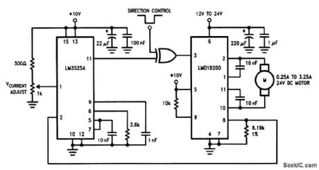
In this circuit, the LM3525 regulating PWM compares the voltage at the current-sense output pin of the LMD18200 with an externally-generated control voltage (VCURRENT ADJUST), and sets the duty cycle of the control signal (from 0 to about 50%) until the motor is running at the desired current level.Switching frequency is about 40 kHz. By inverting the phase of the single control input, the direction of motor rotation can be reversed (View)
View full Circuit Diagram | Comments | Reading(1841)
Electronic hygienical small night lights
Published:2011/8/1 3:05:00 Author:Ecco | Keyword: Electronic, hygienical , small, night lights

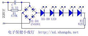
The internal wiring of the lamp is shown as the chart. The 220V mains supply is bucked by capacitor C, rectified by diodes D1-D4 to provide the supply for light emitting diodes D5-D9. LEDs should use green light because green can make people quiet, relaxing. Electronic hygienical small night lights have soft lighting, which is like moon lighting to create a warm and hazy light environment, and it helps people to calm down and fall asleep. In the summer nights, the night light can also give a quiet, cool visual experience.
(View)
View full Circuit Diagram | Comments | Reading(1196)
1500v isolation circuit diagram of D/A convertor
Published:2011/7/30 9:39:00 Author:Sophia | Keyword: D/A convertor, 1500v isolation circuit
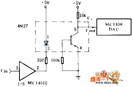
The circuit adopts the Motorola4N27 optical isolator, which provides the required isolation between programmable power D / A converter and CMOS MC1408 non-inverting buffers located far distance. (View)
View full Circuit Diagram | Comments | Reading(679)
VARIABLE_BIPOLAR_CLAMPING
Published:2009/6/29 1:37:00 Author:May
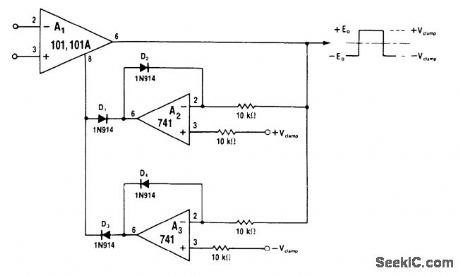
Precision comparator provides independent regulation of both output voltage limits without connection to comparison inputs. A2 and A3 are complementary precision rectifiers having independent positive and negative reference voltages, with both rectifiers operating in dosed loop through A1. A2 senses positive peak of Eo and maintains it equal to +Vclamp by adjusting voltage applied to D1. A3 and D3 perform similar function on negative peaks. Feedback network around output stage of A1 regulatesoutput voltage independently of inputs to A1. —W. G. Jung, IC Op-Amp Cookbook, Howard W. Sams, Indianapolis, IN, 1974, p 228-229. (View)
View full Circuit Diagram | Comments | Reading(932)
High_resolution_dithering_bar_graph_display
Published:2009/7/25 0:15:00 Author:Jessie
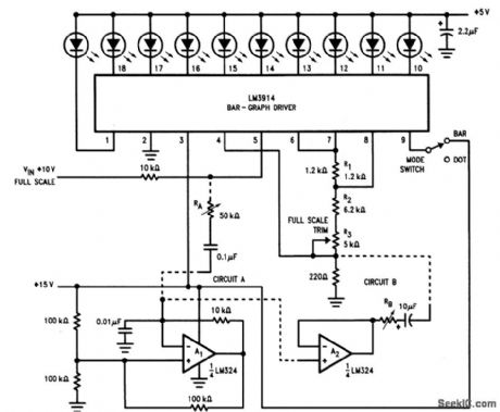
This circuit is an improved version of the Fig. 3-28 display, using a triangular-wave oscillator. With RA properly set, each incremental change in VIN can be detected because the glow from each LED can be made to spread gradually from one device to the next. If the signal-source impedance is high or not linear, false readings might occur. In this case, use CIRCUIT B to buffer the oscillator output. The display is most effective in the dot mode, where supply voltages can be brought up to 15 V. If bar mode is used, do not exceed +5 V on the LEDs (to avoid overheating). To trim, set the LM3914 output to full scale with R3. Then, adjust RA or RB so that when one LED is on, any small measured change of VIN will cause one of the adjacent LEDs to turn on. (View)
View full Circuit Diagram | Comments | Reading(904)
FREQUENCY_PHASE_UP_TO_25_MHz
Published:2009/6/29 1:36:00 Author:May
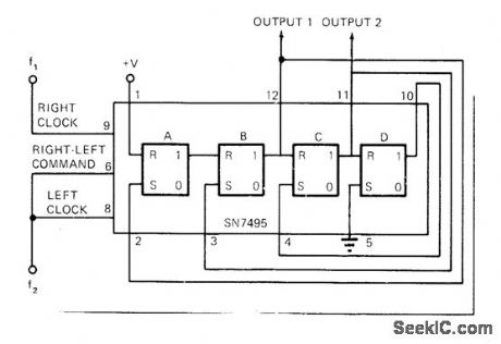
Universal shfft register such as 5495/7495 is connected to compare both frequency and phase of two carier signals anywhere in range from DC to 25 MHz. When f1 is greater than f2, output is 1; when f1 is less than f2, output is 0. For f1 = f2, output is square wave whose duty cycle varies linearly with phase difference between f1 and f2. Comparisons are almost instantaneous, requiring at most two carrier cycles.—J. Breese, Single IC Compares Frequencies and Phase, EDN Magazine, Sept, 15, 1972, p 44. (View)
View full Circuit Diagram | Comments | Reading(1468)
The function circuit of bootstrap circuit
Published:2011/7/29 2:36:00 Author:Sophia | Keyword: bootstrap circuit, function
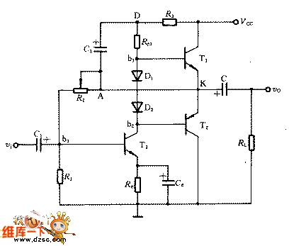
The function of bootstrap circuit
When the circuit is in the static state, , when R3C3 is large enough,VC3doesn't change with vi, actually has no change. So when vi is negative, T1 conducts the electricity,vKwill change from VCC/2 to correct direction. Considering vD=vC3+vK= VC3+vK, obviously, with the rise of electric potential of K spot, D spot electric potential vD will rise automatically. So even if the output voltage amplitude rise very highly, there are enough current iB1 to make theT1 fully conductive. This working is called the bootstrap, which means the circuit itself increase vD.
(View)
View full Circuit Diagram | Comments | Reading(1284)
Dithering_bar_graph_display
Published:2009/7/25 0:13:00 Author:Jessie
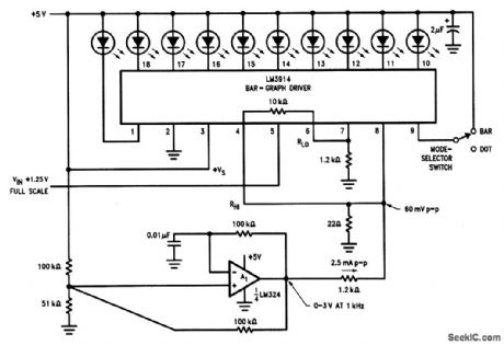
With this circuit, each of 10 LEDs has a fully on and a partially on mode, making 20 states discernible. This is accomplished by the LM324 (operating as a 1-kHz oscillator) driving a 60-mV pp signal into pin 8 of the LM3914.
(View)
View full Circuit Diagram | Comments | Reading(2923)
BASIC_DIGITAL_THERMOMETER_KELVIN_SCALE_WITH_ZERO_ADJUST
Published:2009/6/29 1:35:00 Author:May
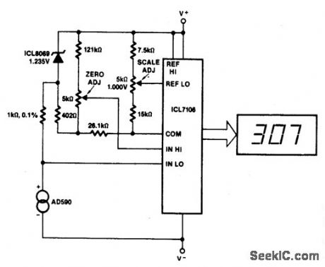
This circuit allows zero adjustment as well as slope adjustment. The ICL8069 brings the input within the common-mode range, while the 5 K pots trim any offset at 218 °K (-55 ℃), and set scale factor. (View)
View full Circuit Diagram | Comments | Reading(1100)
Low_current_ammeter
Published:2009/7/25 0:11:00 Author:Jessie
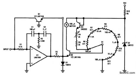
This classic circuit can be updated by substituting an LM11 for the LM216A, an LM194 for the LM114A, and an LM185-1.2 for the LM113. To calibrate, apply a 1-μA input current, and adjust R4 for a full-scale deflection of the 100-μA meter (with S1 set to 1μA). (View)
View full Circuit Diagram | Comments | Reading(2070)
Fast_ac_dc_converter
Published:2009/7/25 0:09:00 Author:Jessie
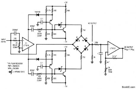
This circuit shows a synchronous-rectifier-based ac/dc converter which has high accuracy up to about 2.5 MHz. To calibrate, apply a 1- to 2-MHz 1-V pp sine wave and adjust the delay compensation so that bridge switching occurs when the sine crosses zero. Next, adjust both skew compensation pots for minimum aberrations in the ac output signal. Finally, adjust the gain trim for a dc output that corresponds to the ac input. (View)
View full Circuit Diagram | Comments | Reading(2554)
BASIC_DIGITAL_THERMOMETER_KELVIN_SCALE
Published:2009/6/29 1:30:00 Author:May
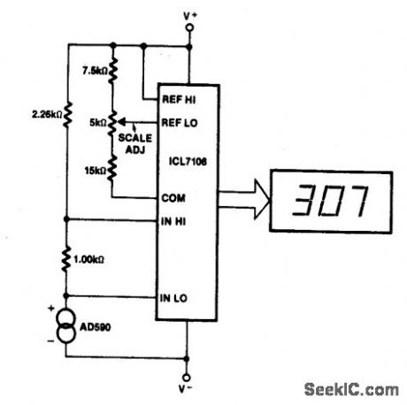
The Kelvin scale vers1on reads from0 to 1999°K theoretically,and from 99Q°K to 473°K actually. The 2.26 K resistor brings themput within the ICL7106 VCM range∶twogeneral-purpose silicon diodes or an LED maybe subsituted. (View)
View full Circuit Diagram | Comments | Reading(1076)
200_ns_sample_hold
Published:2009/7/25 0:07:00 Author:Jessie
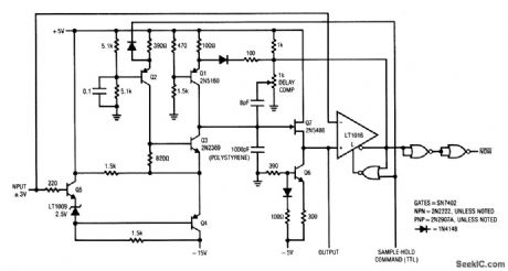
This circuit features an acquisition time of less than 200 ns, a common-mode input range of±3 V, drop of 1μV/pts, hold step of 2 mV, hold settling time of 15 ns, and feedthrough rejection much greater than 100 dB. To calibrate, ground the input, repetitively pulse the sample/hold command line, and adjust the 1-kO pot for 0-V output. (View)
View full Circuit Diagram | Comments | Reading(731)
19_21_V_WINDOW_COMPARATOR
Published:2009/6/29 1:27:00 Author:May
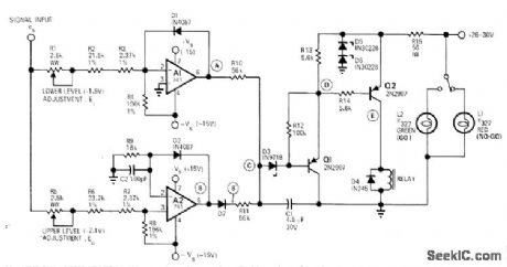
When positive input voltage is between Ievels set by R1 and R5, relay is actuated and green indicator lamp is turned on. Red lamp is on for voltages outside Iimits of window. Article gives design equations and traces operation of circuit. Number of components can be greatly reduced by changing opamps to LM111 comparators.—J.C. Nirschl, 'Window' Comparator Indicates System Status, EDN|EEE Magazine, June 15, 1971, p 49-50. (View)
View full Circuit Diagram | Comments | Reading(779)
INTERNALLY_GATED_WINDOW_COMPARATOR
Published:2009/6/29 1:25:00 Author:May
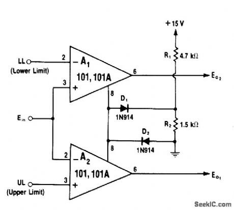
Operation is based on fact that source and sink currents available at pin 8 of 101 opamp are unequal, with negative-going drive being larger. Voltage at pin 8 is low if either comparison input (A1 or A2 so dictates. Both A1 and A2 must have high outputs for pin 8 to be high. Outputs of A1 and A2 thus follow pin 8 since opamps have unity gain. D1 and D2 form clamp network. Either output of A1 or A2 can be used. Outputs go to +5 V only when input voltage is in window established by upper and lower voltage limits.-W. G. Jung, IC Op-Amp Cookbook, Howard W, Sams, Indianapolis, IN, 1974, p 231-232. (View)
View full Circuit Diagram | Comments | Reading(869)
Precision_voltage_inverter
Published:2009/7/25 0:06:00 Author:Jessie
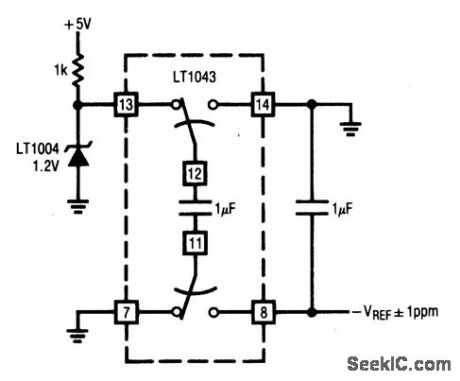
This circuit shows an LTC1043 (Fig. 1-4B) connected as a precision inverter. The circuit allows a reference to be inverted with 1 ppm accuracy. The circuit has high input impedance and requires no trimming. (View)
View full Circuit Diagram | Comments | Reading(0)
STAIRCASE_WINDOW_COMPARATOR
Published:2009/6/29 1:24:00 Author:May
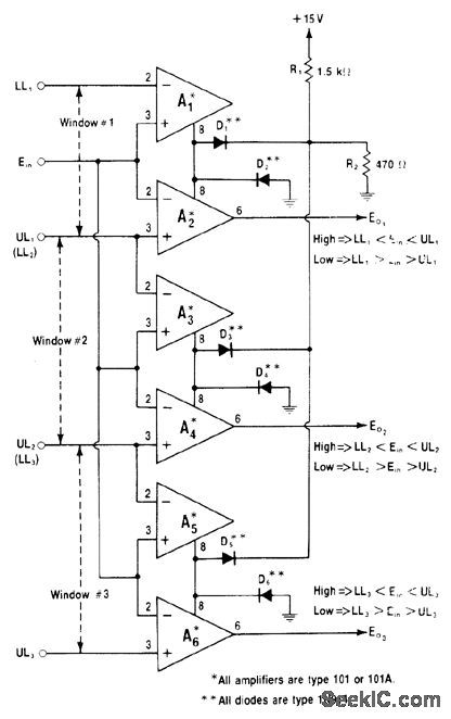
Cascading of 101-type window comparators for sequential operation indicates which of three windows input voltage is in. Input voltage is applied in parallel to all comparators. Output goes high only for comparator whose range includes voltage value of input. Lamp or other indicator can be added to each output line to give visual indication of voltage range.—W. G. Jung, IC Op-Amp Cookbook, Howard W. Sams, Indianapolis, IN, 1974, p 233-234. (View)
View full Circuit Diagram | Comments | Reading(1493)
SOLENOID_DRIVER_
Published:2009/6/29 Author:May
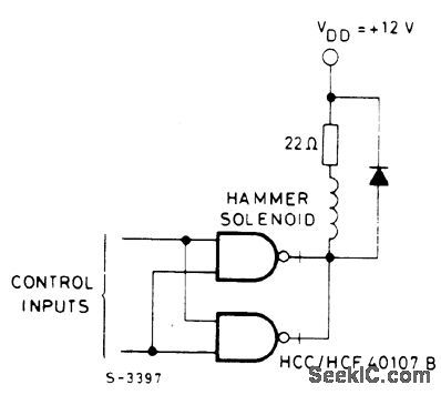
View full Circuit Diagram | Comments | Reading(910)
ADJUSTABLE_FINISH_CHARGE
Published:2009/6/29 Author:May
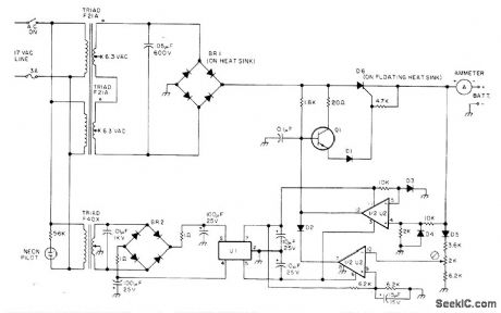
Uses National LM319D dual comparator U2 to sense end-of-charge battery voltage and provide protection against shorted or reversed charger leads. Final charging voltage for 12-V storage batteries is adjustable with 2K trimpot. Separate ±15 V supply using Raytheon RC4195NB regulator U1 is provided for U2. D1-D5 are 1N4002 or HEP-R0051. D6 is 2N682 or HEP-R1471. BR1 is Mo-torola MDA980-2 or HEP-B0876 12-A brldge. BR2 is Varp VE27 1-A bridge. Q1 is 2N3641 or HEP-S0015.-H. Olson, Battery Chargers Exposed, 73 Magazine, Nov. 1976, p 98-100 and 102-104. (View)
View full Circuit Diagram | Comments | Reading(1032)
CRT_YOKE_DRIVER_
Published:2009/6/28 23:59:00 Author:May
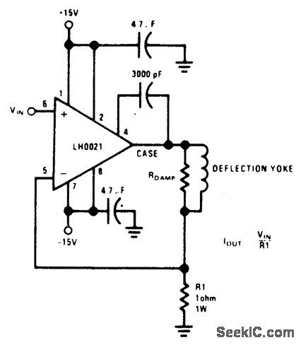
Circuit Notes A 500 mV peak-to-peak triangular waveform about ground is input to the amplifier,gtvmg rlse to a 100 mA peak current to theinductor,. (View)
View full Circuit Diagram | Comments | Reading(1005)
| Pages:1258/2234 At 2012411242124312441245124612471248124912501251125212531254125512561257125812591260Under 20 |
Circuit Categories
power supply circuit
Amplifier Circuit
Basic Circuit
LED and Light Circuit
Sensor Circuit
Signal Processing
Electrical Equipment Circuit
Control Circuit
Remote Control Circuit
A/D-D/A Converter Circuit
Audio Circuit
Measuring and Test Circuit
Communication Circuit
Computer-Related Circuit
555 Circuit
Automotive Circuit
Repairing Circuit