
Circuit Diagram
Index 1252
Tachless_motor_speed_controller
Published:2009/7/24 23:28:00 Author:Jessie
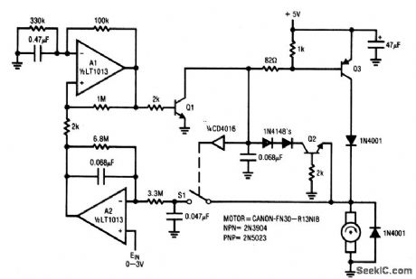
This circuit is particularly applicable to digitally controlled systems in robotic and X-Y positioning applications. The circuit controls from 20 rpm to full speed (with good transient response under all shaft conditions) by sensing the motor's back EMF to determine speed. The difference between the speed and a setpoint is used to close a sampled loop around the motor. A1 generates a pulse train. When the A1 output is high, Q1 is biased, Q3 turns off, and the motor back EMF appears after the inductive flyback stops, During this period, the S1 (a switch within the CD4016) input is turned on, and the 0.047-μF capacitor charges to the back EMF value. A2 compares this value with the setpoint, and the amplifier difference changes the A1 duty cycle, thus controlling motor speed. The setpoint is controlled by a -3-V signal (Ein) at the A2 noninverting input. (View)
View full Circuit Diagram | Comments | Reading(2190)
Push-pull converter circuit diagram composed of TDA4718
Published:2011/8/1 2:48:00 Author:Ecco | Keyword: Push-pull converter

The push-pull converter circuit composed of TDA4718 is shown as the chart. It uses two switching elements to do on / off work and to prevent the transformer magnetic saturation, then it can increase conversion efficiency. Transformer windings N1, N2 and N3, N4 are not symmetrical around system, and the bias point of the hysteresis loop will move, that is magnetic bias, then the output voltage increase will result in saturation. Because the transformer windings will produce stray capacitance, therefore, the higher the frequency will result in more complex inductive coupling effect between wingings.
(View)
View full Circuit Diagram | Comments | Reading(5216)
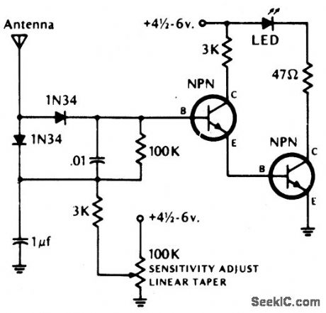
ADJUSTABLE_SENSITIVITY_FIELD_STRENGTH_INDICATOR
Published:2009/6/29 2:24:00 Author:May
Circuit Notes
The LED lights if the rf field is higher than the pre-set field strength level. Diodes should be germanium. Transistors (NPN) = 2N2222, 2N3393, 2N3904 or equivalent. (View)
View full Circuit Diagram | Comments | Reading(3617)
Power_op_amp_bridge_amplifier_with_differential_output
Published:2009/7/24 23:27:00 Author:Jessie
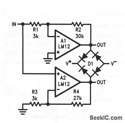
The differential output of the LM12 (Fig. 10-46) amplifier almost doubles the voltage swing delivered to the load. The diodes clamp the outputs to the supplies. (View)
View full Circuit Diagram | Comments | Reading(1060)
MEASURING_THRESHOLDS
Published:2009/6/29 2:23:00 Author:May
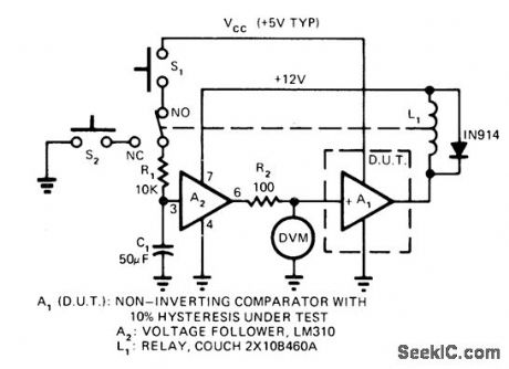
Upper and lower thresholds of noninverting comparator under test (A1) are read on DVM at end of capacitor charge and discharge cycles initiated by S1 and S2. With C1 discharged, relay L1 is energized. Closing S1 allows C1 to charge toward VCC. When upper threshold is reached, relay drops out and meter is read. Closing S2 starts discharge cycle which stops at lower threshold. Reverse relay connections when testing inverting comparator.—E. S. Papanicolaou, Comparator is Part of its Own Measuring System, EON Magazine, Aug. 5, 1974, p 76. (View)
View full Circuit Diagram | Comments | Reading(734)
Ultra_precision_instrumentation_amplifier
Published:2009/7/24 23:26:00 Author:Jessie
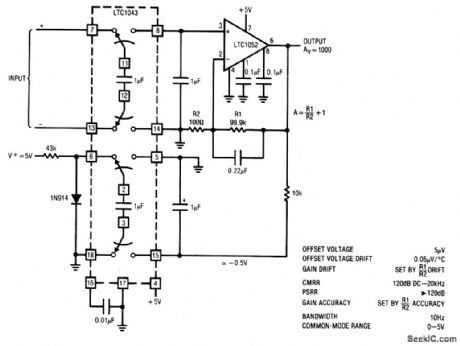
This circuit provides greater precision than that of the circuit in Fig. 3-4, but at the expense of bandwidth, as shown by the corresponding table. (View)
View full Circuit Diagram | Comments | Reading(0)
SEQUENTIAL_UJT_TIMER
Published:2009/6/29 2:22:00 Author:May
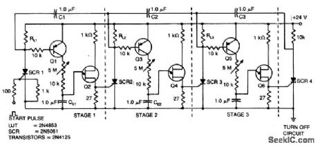
View full Circuit Diagram | Comments | Reading(640)
Power_op_amp_with_single_supply_operation
Published:2009/7/24 23:26:00 Author:Jessie
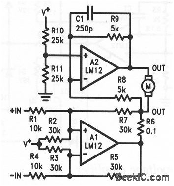
The output current of the LM12 (Fig. 10-46) bridged amplifier is proportional to differential-input voltage, thus eliminating the need for two supplies. If the output is a motor load (as shown), use output clamp diodes. (View)
View full Circuit Diagram | Comments | Reading(774)
SEQUENTIAL_TIMER_1
Published:2009/6/29 2:21:00 Author:May
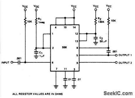
By utilizing both halves of a dual timer it is possible to obtain sequential timing. By connecting the output of the first half to the input of the second half via a.001μF coupling capacitor sequential timing may be obtained. Delay t1 is determined by the first half and t2 by the second half delay. The first halfof the timer is started by momentarily connecting pin 6 to ground. When it is turned out (determined by 1.1R1C1), the second half begins. Its duration is determined by 1.1R2C2. (View)
View full Circuit Diagram | Comments | Reading(1161)
SENSITIVE_FIELD_STRENGTH_METER
Published:2009/6/29 2:18:00 Author:May
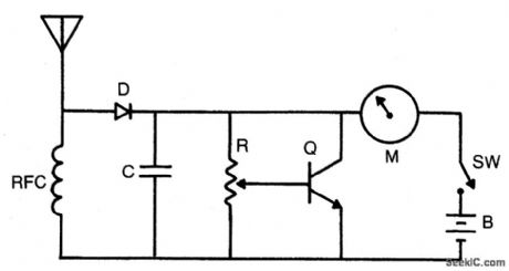
Circuit Notes
Increased sensitivity gives field strength reading from low power transmitters. Operat-ing range 3-30 MHz. To operate, adjust R for 1/3 to 1/2 scale reading. RFC = 2.5 mH choke, C =1.000 pF, R = 50 K pot, M = 0-1 mA, D = 1N34 or 1N60 (Germanium), Q = NPN (RCASK3020, 2N3904 or equivalent). (View)
View full Circuit Diagram | Comments | Reading(3)
10_W_CLASS_A
Published:2009/6/29 2:17:00 Author:May
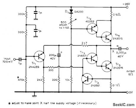
Highly stable circuit uses easily obtainable components. Transistor types are not critical. Shortdrcuit protection is provided by constantcurrent source D1-Tr2-Tr5-Tr4. Output transistors Tr5 and Tr6 requirb heatsinks ca pable of dissipating at least four times rated output power. D1 and Tr2 should be in thermal contact.-A. H. Calvert, Class A Power Ampli-fier, Wireless World, June 1976, p 71. (View)
View full Circuit Diagram | Comments | Reading(1098)
CURRENT_CONTROL_FOR_POWER_SWlTCH
Published:2009/6/29 2:15:00 Author:May
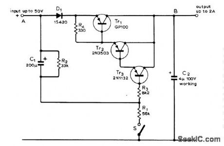
Circuit makes power supply current increase gradually from zero when supply is tumed on, to eliminate transients that sometimes cause alarming loudspeaker thumps in audio systems. Current through silicon power diode D1 is controlled by voltage on C1, which charges up after closing of switch with time constant C1R2R3/(R1 + R2). When switch is opened, rundown of supply curent is controlled by discharge of C1 through R2. Article also covers use of two current control circuits in tandem for handling higher Ioads.-P. J. Briody, Power Supply Delayed Switching, Wireless World, March 1975, p 139-141. (View)
View full Circuit Diagram | Comments | Reading(1132)
3_W_DIFFERENTIAL
Published:2009/6/29 2:14:00 Author:May
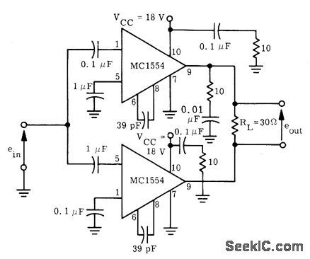
Upper Motorola MC1554 power amplifier is connected in standard configuration for noninverting gain of 9, while lower IC has inverting gain of 9 to give effective overall voltage gain of 18. Input impedance of upper amplifier is 10K while that of lower amplifier is 1K, with unequal input coupling capacitors providing required match of frequency responses. Differential output connection allows output voltage swing to exceed powersupply voltage.- The MC1554 One-Watt Monolithic Integrated Circuit Power Amplifier, Motorola, Phoenix, AZ, 1972, AN-401 p 4 (View)
View full Circuit Diagram | Comments | Reading(731)
LOW_COST_MICROWAVE_FIELD_STRENGTH_METER
Published:2009/6/29 2:13:00 Author:May
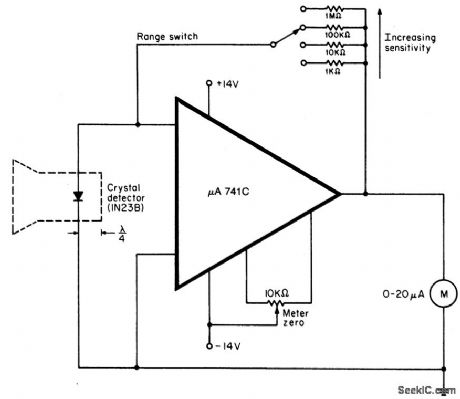
Circuit Notes
When operating, a waveguide directs energy onto a crystal detector. The diode I shown is for X-band operation. The waveguide is a 1 1/2 inch piece of plastic tubing with the ends flared. The plastic is coated with an electroless copper solution to provide a conducting surface. The dimensions are not critical. For calibrated readings, the meter is placed in a known field or else compared to a calibrated meter. To operate the meter, point it away from the signal. Switch the meter to the de-sired range, and adjust the zero control for a 0 reading. Then point the waveguide at the sig-nal, and read field strength directly. (View)
View full Circuit Diagram | Comments | Reading(737)
Pozoer_op_amp_servo_amplifier_rate_generator
Published:2009/7/24 23:36:00 Author:Jessie
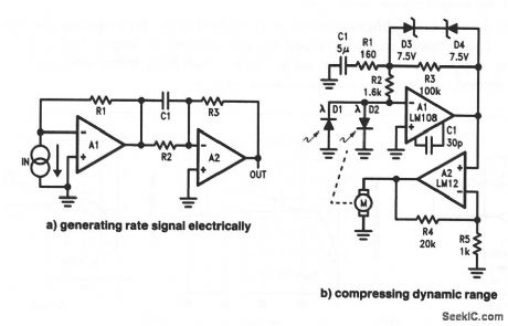
This servo provides an output speed that is proportional to the input voltage, but with a rate signal to compress the dynamic range. This is done electrically by differentiating the servo error signal (as shown in Fig. 10-57A). The LM12 (Fig. 10-46) provides current drive to the motor. (View)
View full Circuit Diagram | Comments | Reading(892)
FET_PREAMP_WITH_TONE_CONTROLS
Published:2009/6/29 2:13:00 Author:May
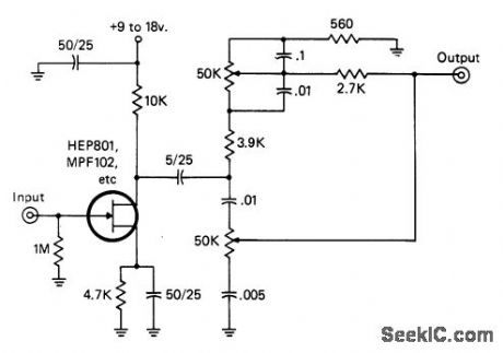
Developed for use with simple 2-W audio amplifier when testing very low-level output circuits and microphones. Will not load circuit to which input is connected. Optional bass/treble tone controls are included.-J. Schultz, An Audio Circuit Breadboarder's Delight, CQ Jan. 1978, p 42 and 75. (View)
View full Circuit Diagram | Comments | Reading(1566)
5_V_from_four_cells_linear_regulation
Published:2009/7/24 23:35:00 Author:Jessie
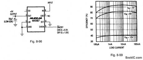
Figure 8-98 shows a MAX667 linear regulator connected to provide a 5-V output from four cells. The input voltage range is 4 V to 16.5 V. The quiescent current (VIN = 6 V) is 10 μA, and the maximum load current (VIN = 6 V) is 250 mA. The dropout voltage is 100 mV with a 100-mA load. Figure 8-99 shows the efficiency curves. MAXIM BATTERY MANAGEMENT CIRCUIT COLLECTION, 1994, P. 21.
(View)
View full Circuit Diagram | Comments | Reading(645)
THREE_LEVEL_COMPARATOR
Published:2009/6/29 2:12:00 Author:May
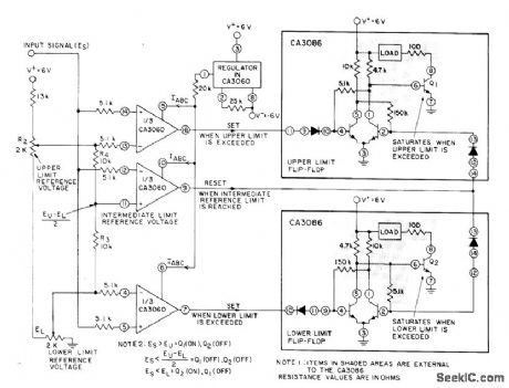
All three sections of CA3060 three-opamp array are used with CA3086 transistor arrays to provide three adjustable limits for comparator. If upprr orlower limit is exceeded, appropriate output is types of industrial control pplications.— Ciractivated until input signal retums to presecuit ideas for RCA Linear ICs, RCA Solid State lected intermediate limit. Suitable for many Division, Somerville, NJ, 1977, p 17. (View)
View full Circuit Diagram | Comments | Reading(2008)
FSK_decoding_with_carrier_detect
Published:2009/7/24 23:35:00 Author:Jessie

This circuit is similar to that of Fig. 3-9, but it also uses the lock-detect section of the XR-2211 (Fig. 3-9C) as a carrier-detect option for FSK decoding. The lock-detect output at pin 6 is shorted to the data output at pin 7. The data output is disabled in the low state until there is a carrier within the detection band of the PLL, and pin 6 goes high to enable the data output. The minimum value of lock-detect filter capacitance CD (pins 3 and 4) can be calculated using: CD (inμF)=16/capture range in Hz. Large values of CD slow response time of the lock-detect output, and small CD values can result in chatter on the lock-detect output as an incoming signal approaches the capture-bandwidth frequency. (View)
View full Circuit Diagram | Comments | Reading(2212)
STROBED_MICROPOWER
Published:2009/6/29 2:12:00 Author:May
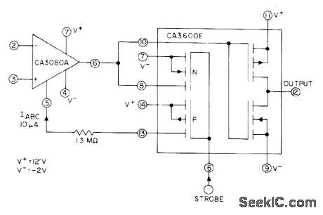
Uses CA3080A var-iable opamp and CA3600E CMOS transistor array. Quiescent power drain from ±12V supply is only 10 μW, increasing to 420 μW when comparator is strobed on to make CA3080A active.— Circuit ideas for RCA Linear ICs, RCA Solid State Division, Somerville, NJ, 1977, p 16. (View)
View full Circuit Diagram | Comments | Reading(749)
| Pages:1252/2234 At 2012411242124312441245124612471248124912501251125212531254125512561257125812591260Under 20 |
Circuit Categories
power supply circuit
Amplifier Circuit
Basic Circuit
LED and Light Circuit
Sensor Circuit
Signal Processing
Electrical Equipment Circuit
Control Circuit
Remote Control Circuit
A/D-D/A Converter Circuit
Audio Circuit
Measuring and Test Circuit
Communication Circuit
Computer-Related Circuit
555 Circuit
Automotive Circuit
Repairing Circuit