
Circuit Diagram
Index 1253
COMPARATOR_DRIVES_LAMP
Published:2009/6/29 2:11:00 Author:May
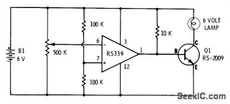
Classroom demonstration circuit for comparator action uses transistor to amplify output of one section of RS339 quad comparator, to boost output currnet rent enough for driving 60-mA lamp. Lamp comes on when voltage at movablearm of 500K pot is greater than half of supply voltage.—F.M. Mims, Integrated Cireuit Projects, Vol. 6, Radio Shack, Fort Worth, TX, 1977, p 33-41. (View)
View full Circuit Diagram | Comments | Reading(666)
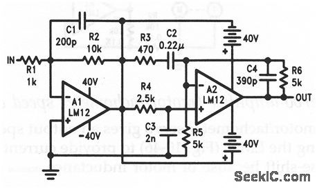
Power_op_amp_servo_amplifier_motor_tachometer_speed_control
Published:2009/7/24 23:35:00 Author:Jessie
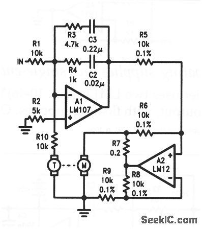
This motor/tachometer servo gives an output speed proportional to input voltage. Using the LM12 (Fig. 10-46) to provide current drive to the motor reduces loop phase-shift because of motor inductance. (View)
View full Circuit Diagram | Comments | Reading(942)
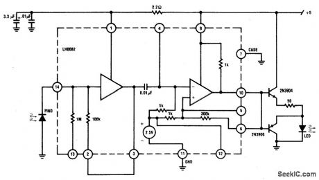
FIBER_OPTIC_RECEIVER,LOW_SENSITIVITY,2μW
Published:2009/6/29 2:08:00 Author:May

View full Circuit Diagram | Comments | Reading(622)
Power_op_amp_audio_amplifier
Published:2009/7/24 23:34:00 Author:Jessie
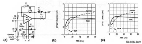
This amplifier uses a single LM12 (Fig. 10-46) with dual supplies. Figure 10-55B shows the total harmonic distortion or THD (Fig. 1-E) for both low-and high-level outputs. Typical intermodulation distortion (Fig. 1-F) is 0.015% with ±10 V into a 4-Ω load, using the standard 60-Hz/7-kHz 4:1 test conditions. Figure 10-55C shows the offset-voltage change after the application of a load that dissipates 50 W in each output transistor. (View)
View full Circuit Diagram | Comments | Reading(729)
Frequency_shift_decoder_FSK
Published:2009/7/24 23:34:00 Author:Jessie
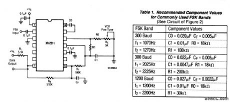
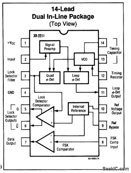

This circuit shows an XR-2211 connected for FSK decoding. Recommended component values for some of the most commonly used FSK bands are given in Fig. 3-9B. Internal functions of the XR-2211 are given in Fig. 3-9C. The.circuit can be tailored for any FSK-decoding application by the choice of R0, R1,C0, C1, and CF. For a given set of FSK mark and space frequencies, f1 and f2, these parameters can be calculated as follows: Calculate PLL center frequency fo using:
Use 18 kΩ for R0 so that R0 can be set to 20 kΩ with the series Rx pot. Calculate the value of C0 using: C0=1/R0f0.Calculate R1 to give a difference frequency equal to the mark-space deviation: R1= R0[(f0/f1--/f2)].Calculate C1 (which sets the loop-filter time constant) using: C1= C0/4.Calculate CF (which is the data-filter capacitance with RF=100 kΩ and RF= 510 kΩ) using: CF (inμF) =3/baud rate.
All calculated values, value. except R0, can be rounded off to the nearest standard walue .R0 can be fine tuned with Rx. (View)
View full Circuit Diagram | Comments | Reading(1480)
SEQUENTIAL_TIMER
Published:2009/6/29 2:07:00 Author:May
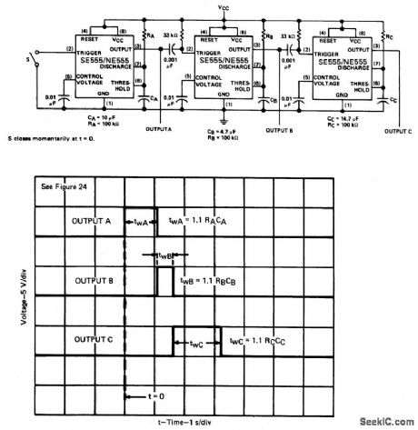
Many applications, such as computers, re-quire signals for initializing conditions during start-up. Other applications such as test equipment require activation of test signals in sequence. SE555/NE555 circuits may be connected to provide such sequential control. The timers may be used in various combinations of astable or monostable circuit connections, with or without modulation, for extremely flexible waveform control. (View)
View full Circuit Diagram | Comments | Reading(355)
FIBER_OPTIC_RECEIVER,HIGH_SENSITIVITY,30nW
Published:2009/6/29 2:07:00 Author:May
View full Circuit Diagram | Comments | Reading(732)
33_Vfrom_four_to_six_cells
Published:2009/7/24 23:33:00 Author:Jessie
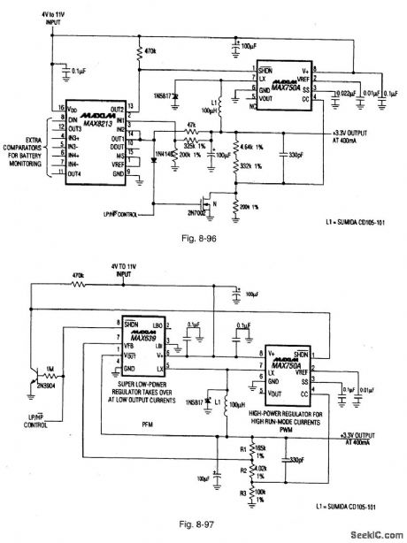
Figures 8-96 and 8-97 show two circuits that provide 3.3 V with four- to six-cell inputs. Both circuits can be switched (by an LP/HP control signal) between high-and low-power modes to accommodate equipment that operates in two modes. The circuit of Fig. 8-96 has a quiescent current of 60 μA (VIN = 4.8 V) in the LP mode and 1.6 mA in the HP mode. Maximum load current (VIN = 4 V) in LP is 10 mA, and 400 mA in HP. Efficiency (VIN = 4.8 V) in LP is 72%, with a 1-mA load, and 92% in HP, with a 100-mA load. The circuit of Fig. 8-97 has a quiescent current (VIN = 4.8 V) in the LP mode of 25 pA and 1.6-mA in HP. The maximum load current (VIN = 4 V) in LP is 50 mA, and 400 mA in HP. Efficiency (VIN = 4.8 V) in LP is 86%, with a 1-mA load, and 92% in HP, with a 100-mA load. MAXIM BATTERY MANAGEMENT CIRCUIT COLLECTION, 1994, P. 17. (View)
View full Circuit Diagram | Comments | Reading(612)
DIRECT_COUPLED_PUSH_PULL
Published:2009/6/29 2:06:00 Author:May
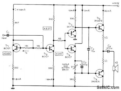
Provides highquality sound at ample volume for car radio, operating from 9.3-V regulated supply. Pushpull emitter-follower stages are connected to give symmetrical low output impedance on both positive and negative portions of audio waveform. Input transistor Tr1 provides tomperature compensation, while driver Tr2 providos temperature-compensated bias and maximum symmetrical voltage swings to output stages.-G. Kalanit, Low Voltage Audio Ampli fier, Wireless World, Oct, 1976, p 74. (View)
View full Circuit Diagram | Comments | Reading(1552)
THUMBWHEEL_PROGRAMMABLE_INTERVAL_TIMER
Published:2009/6/29 2:06:00 Author:May
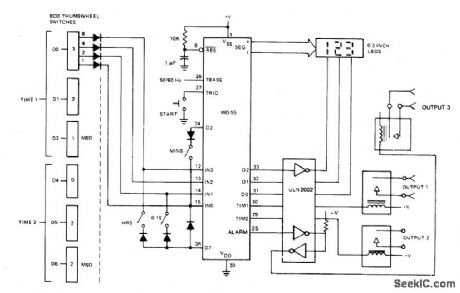
Switch programmable on/off or interval timer, has three relay-switched outputs. 0ut-put one is active for the duration of time 1, output two is active for the duration of time 2, and output three is active for the duration of both one and two. Timing data is input through 6 BCD-encoded thumbwheel switches. Three SPST switches inform the WD-55 to interpret this data as NNN seconds. NNN seconds, NNN minutes, or NNN hours. The LED display will show the time remaining and the countdown when operating. Since the data is input through switches, the display may be deleted. Also, since the timing information is read from switches, the data is nonvolatile and no battery backup is required. (View)
View full Circuit Diagram | Comments | Reading(1426)
Power_op_amp_cascade_amplifier
Published:2009/7/24 23:32:00 Author:Jessie
This amplifier cascades two LM12s (Fig. 10-46) to double the output swing. The output can be increased by any number of stages, but a separate floating supply is required for each. Notice that both input and output are single-ended. (View)
View full Circuit Diagram | Comments | Reading(833)
Power_op_amp_with_floating_supplies_and_single_ended_output
Published:2009/7/24 23:31:00 Author:Jessie
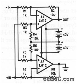
This amplifier uses two LM12s (Fig. 10-46) to provide a differential input, but single-ended output, with floating supplies. Output swing is ±70 V at ±10A. (View)
View full Circuit Diagram | Comments | Reading(808)
FIBER_OPTIC_LINK_REPEATER
Published:2009/6/29 2:06:00 Author:May
View full Circuit Diagram | Comments | Reading(962)
One_hour_timer_with_manual_controls
Published:2009/7/24 23:30:00 Author:Jessie
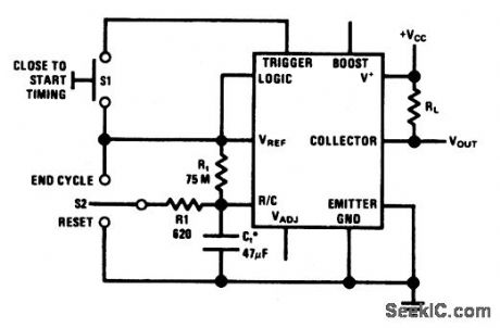
This circuit uses an LM122 connected as a one-hour timer with manual controls for start, reset and cycle-end. S1 starts timing, but has no effect after timing has started. S2 is a center-off switch, which can either end the cycle prematurely or reset to 0 V. A new timing period starts as soon as S2 is released from the reset position. The average charging current through R1 is about 30 nA, so you must pay some attention to the parts layout to prevent stray leakage paths.The suggested timing capacitor has a typical self-time constant of 300 hours, and a guaranteed minimum of 25 hours at + 25℃. (View)
View full Circuit Diagram | Comments | Reading(858)
60_W
Published:2009/6/29 2:05:00 Author:May
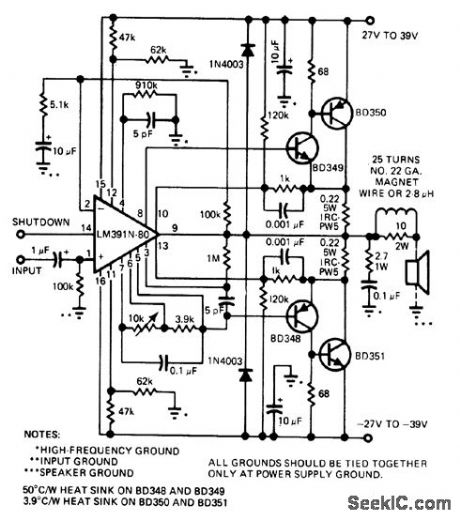
Combination of National LM391 audio driver 10 and discrete power transistors provides 60-W output for loudspeaker at very low distortion. IC output can swing ±40V.Totalharmonic distortion of circuit is under 0.05%.-P.Franson, Consumer-Product IC's-New Offerings Trtgger an Explosion in Markets Old and New,EDN Magazine, Nov.5,1977,p 54-65. (View)
View full Circuit Diagram | Comments | Reading(2697)
4__to_20_mA_current_loop_transmitter
Published:2009/7/24 23:30:00 Author:Jessie
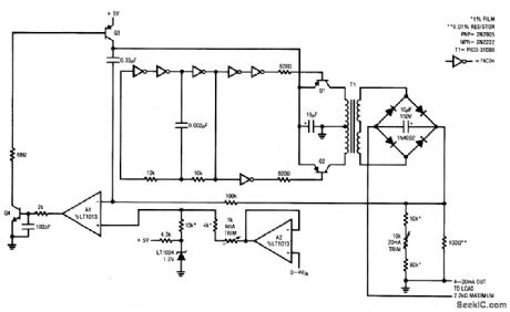
This circuit transmits an industry standard 4-20 mA current loop signal to valves and other actuators. The 5-V circuit uses a servo-controlled dc/dc converter to generate the compliance voltage necessary for loop-current requirements (the circuit will drive 4 to 20 mA into loads as high as 2.2 kΩ, or 44-V compliance, and is inherently short-circuit protected). To calibrate, short the output, apply 0 V to the input, and adjust the 4-mA trim for 0.3996 V across the 100-Ω resistor. Next, increase the input to 4.000V and trim the 20-mA adjustment for 1.998 V across the 100-Ωresistor. Repeat this procedure until both points are fixed. The gain-trim network shunting the 100-Ω resistor requires the odd voltage-trim target values (1.998 and 0.3996). However, the output current swings between 4.000 and 20.00 mA, when the input voltage is varied between 0 V and 4V. (View)
View full Circuit Diagram | Comments | Reading(1954)
BATTERYLESS_MICROPHONE_PREAMP
Published:2009/6/29 2:04:00 Author:May
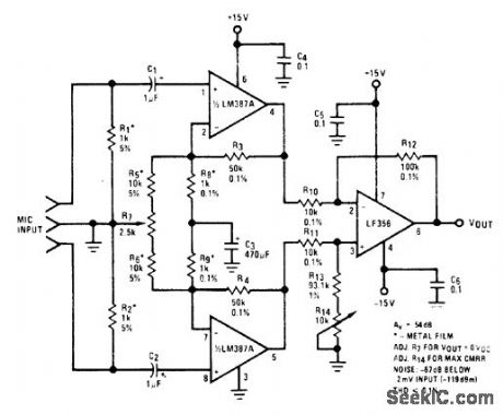
Transistor and two components can be mounted in microphone housing. R2 is added to existing amplifier to provide operating voltage for preamp, while C2 feeds preamp signal to input of amplifier.-W. H. Jarvis, Line-Powered Mi-crophone Pre-Amp, Wireless World, Dec. 1976, p 43. (View)
View full Circuit Diagram | Comments | Reading(1454)
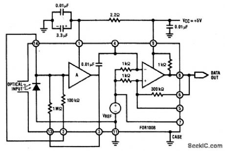
FIBER_OPTIC_LINK
Published:2009/6/29 2:04:00 Author:May
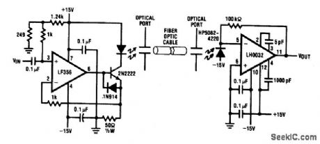
Circuit Notes
Fiber Optic applications require analog drivers and receivers operating in the megahertz region. This complete analog transmission system is suitable for optical communication applications up to 3.5 MHz.The transmitter LED is normally biased at 50 mA operating current. The input is capacitively coupled and ranges from 0 to 5 \I, modulating the LED current from 0 to 100 mA. The re-ceiver circuit is configured as a transimpe-dance amplifier. The photodiode with 0.5 amp per watt responsivity generates a 50 mV signal at the receiver output for 1,u,W of light input. (View)
View full Circuit Diagram | Comments | Reading(2)
Power_op_amyo_high_voltage_amplifier
Published:2009/7/24 23:29:00 Author:Jessie
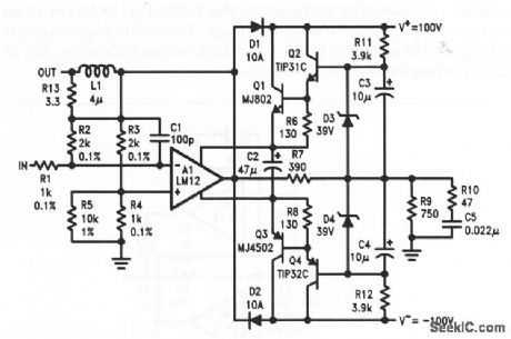
This amplifier can drive ±90 V at 10 A, more than twice the output swing of the LM12 (Fig. 10-46), which provides both current and power limiting for the discrete transistors. (View)
View full Circuit Diagram | Comments | Reading(5532)
FAHRENHEIT_THERMOMETER
Published:2009/6/29 2:03:00 Author:May
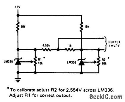
View full Circuit Diagram | Comments | Reading(1091)
| Pages:1253/2234 At 2012411242124312441245124612471248124912501251125212531254125512561257125812591260Under 20 |
Circuit Categories
power supply circuit
Amplifier Circuit
Basic Circuit
LED and Light Circuit
Sensor Circuit
Signal Processing
Electrical Equipment Circuit
Control Circuit
Remote Control Circuit
A/D-D/A Converter Circuit
Audio Circuit
Measuring and Test Circuit
Communication Circuit
Computer-Related Circuit
555 Circuit
Automotive Circuit
Repairing Circuit