
Circuit Diagram
Index 1240
Inverting_amplifier_with_high_input_impedance
Published:2009/7/24 21:13:00 Author:Jessie
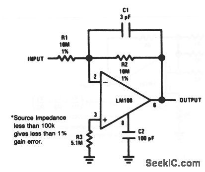
This circuit provides an input impedance of about 10 MΩ. C1 is necessary to provide stabilization feedback. C2 compensates for frequency shift caused by C1. (View)
View full Circuit Diagram | Comments | Reading(872)
Noninverting_summing_amplifier
Published:2009/7/24 21:12:00 Author:Jessie
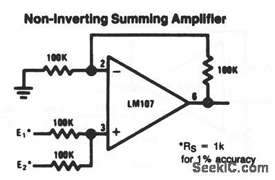
This circuit shows an LM107 in the classic noninverting summing-amplifier configuration, where VOUT depends on the sum of the input voltages (E1, E2), with all resistors at the same value. The accuracy of the circuit depends on the input-voltage source resistance (and will be 1% if the source is 1 kΩ). (View)
View full Circuit Diagram | Comments | Reading(1144)
Inverting_summing_amplifier
Published:2009/7/24 21:11:00 Author:Jessie
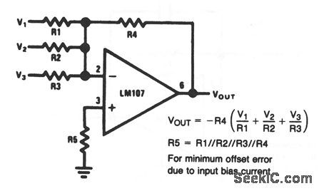
This circuit shows an LM107 in the classic inverting summing amplifier configuration, where VOUT depends on the sum of the input voltages(V1,V2,V3), as well as the ratios of R1 through R4. As shown, offset error is minimum when R5 equals the parallel resistance of R1 through R4. (View)
View full Circuit Diagram | Comments | Reading(0)
High_power_booster
Published:2009/7/24 21:10:00 Author:Jessie

Figure 5-39 is a 1-A version of the Fig. 5-36 circuit. Figure 5-40 shows the waveforms for a 10-V negative input step (trace A) with a 10-Ω, load. The amplifier responds (trace B) driving the booster to close the loop. The booster output, lagging by nanoseconds (trace C), drives the load with only minor peaking (which can be minimized with the feedback capacitance trimmer). LINEAR TECHNOLOGY, APPLICATION NOTE 47, P. 47. (View)
View full Circuit Diagram | Comments | Reading(1008)
Difference_amplifier
Published:2009/7/24 21:09:00 Author:Jessie
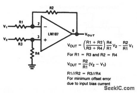
This circuit shows an LM107 in the classic difference-amplifier configuration, where VOUT depends on the difference between V1 and V2, as well as the ratios of R1 through R4. As shown, the calculations for VOUT are simplified when R1=R3 and R2=R4. (View)
View full Circuit Diagram | Comments | Reading(0)
Power_booster
Published:2009/7/24 21:08:00 Author:Jessie
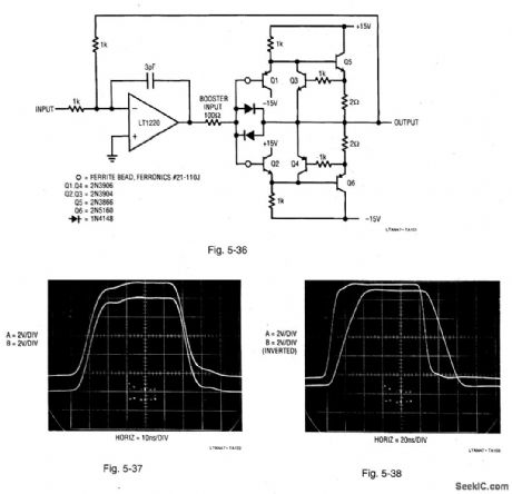
Figure 5-36 shows a 200-mA power booster used with an LT1220 amplifier. Figure 5-37 shows booster performance with the LT1220 removed. The input pulse (trace A) is applied to the booster input, with the output (trace B) taken at the indicated point. The total delay is about 1 ns. Figure 5-38 shows pulse response with the LT1220 installed and a 50-Ω load. The input (trace A) produces a slew-limited output (trace B). LINEAR TECHNOLOGY, APPLICATION NOTE 47, P. 46. (View)
View full Circuit Diagram | Comments | Reading(1)
THREE_AMPLIFIER_ACTIVE_FILTER
Published:2009/6/29 21:48:00 Author:May
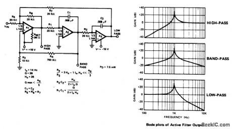
Circuit NotesThe active filter is a state variable filter with bandpass, high-pass and low-pass outputs, It is a classical analog computer method of implementing a filter using three amplifiers and only two capacitors. (View)
View full Circuit Diagram | Comments | Reading(1113)
SERIAL_DATA_OUTPUT
Published:2009/6/29 21:48:00 Author:May
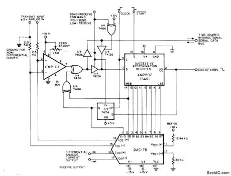
Precision Monolithics ICs form transceiving converter suitable for use in control systems incorporating 8-bit microprocessors. Output conforms whh Bell-System μ-255 logarithmic law for PCM transmission. Applications include servocontrols, stress and vibration analysis, digital recording, and speech synthesis. Start must be held low for one clock cycle to begin send or receive cycle. Conversion is completed in nine dock cycles, and output is available for one full clock cycle,Other half of system is identical.— COMDAC Companding D/A Convener, Precision Monolithics、Santa Clara、CA,1977、DAC-76、p 12 (View)
View full Circuit Diagram | Comments | Reading(1220)
SALLEN_KEY_SECOND_ORDER_LOW_PASS_FILTER
Published:2009/6/29 21:47:00 Author:May
View full Circuit Diagram | Comments | Reading(714)
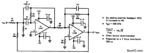
MFB_BANDPASS_FILTER_FOR_MULTICHANNEL_TONE_DECODER
Published:2009/6/29 21:44:00 Author:May
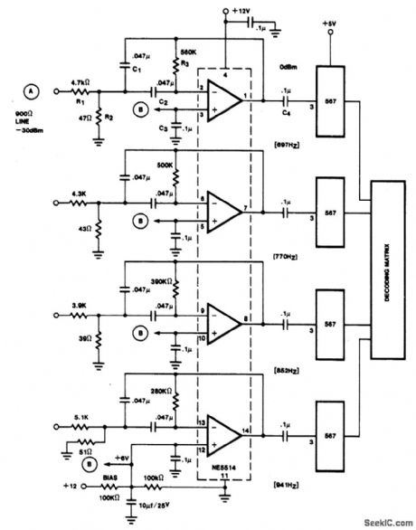
View full Circuit Diagram | Comments | Reading(733)
Finger Touch Induction Switch Circuit
Published:2011/7/21 10:06:00 Author:Joyce | Keyword: Finger , Touch , Induction, Switch
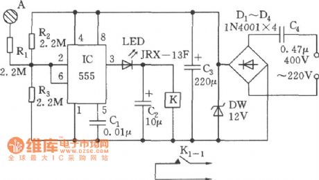
As shown in the figure, this circuit is composed of a depressurization and rectification circuit and a 555 trigger. When a hand touches the metal A, the induction signal will turn the comparator within 555 to set, K will be actuated and contact K1-1 will close; another trigger of A will release K and, disconnect K1-1. (View)
View full Circuit Diagram | Comments | Reading(1183)
One-button Biostable Switch Circuit
Published:2011/7/21 10:21:00 Author:Joyce | Keyword: One-button , Biostable , Switch
As shown in the figure, 555 is the core of the circuit. Pay attention that R1 = R2 = 47 k Ω and the trigger end feet 2 (set ) connected to 555 and the threshold level end feet 6 (reset); Resistance R3, capacitance C2 for charge and discharge are connected to the output end feet3, and are linked with feet 2 and 6 through the switch. When S disconnects, feet 2, 6 are both 1/2 VDD = 6 V, therefore, the level of feet is random, sometimes it is high, and sometimes it is low. If feet 3 is a high level (about VDD-1. 5 V = 10.5 V), pressing S will add the charge voltage on C2 to feet 6 , to make it higher than trigger level 2/3 VDD, then 555 will be reset, and feet3 will become a low level. (View)
View full Circuit Diagram | Comments | Reading(1336)
Single_op_amp_full_wave_rectifier
Published:2009/7/24 21:37:00 Author:Jessie
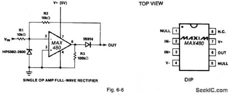
Figure 6-6 shows a MAX480 connected to form a full-wave rectifier. Maximum offset-voltage drift is 1.5 μV/℃, maximum supply current is 20 μA, minimum output drive is 5 mA, maximum input-offset voltage is 70 μV, maximum input bias current is 3 nA, and minimum open-loop gain is 700 V/mV. MAXIM NEW RELEASES DATA BOOK, 1993, P. 3-23. (View)
View full Circuit Diagram | Comments | Reading(0)
Op_amp_function_generator
Published:2009/7/24 21:36:00 Author:Jessie
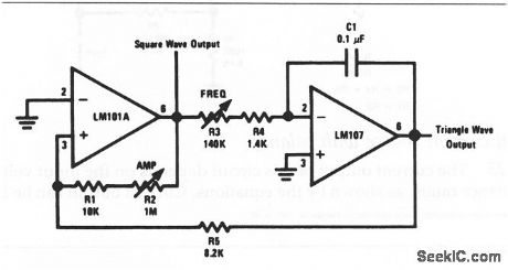
This circuit is the op-amp version of the classic sine/triangle function generator (chapter 5). Notice that both frequency and amplitude are adjustable. (View)
View full Circuit Diagram | Comments | Reading(1906)
Cable_driver_with_minimum_phase_distortion
Published:2009/7/24 21:36:00 Author:Jessie
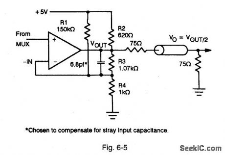
Figure 6-5 shows how the circuits of Figs. 6-3 and 6-4 can be connected to provide minimum phase distortion. MAXIM NEW RELEASES DATA Book, 1993, P. 3-20. (View)
View full Circuit Diagram | Comments | Reading(735)
Op_amp_Wien_bridge_sine_wave_oscillator
Published:2009/7/24 21:35:00 Author:Jessie
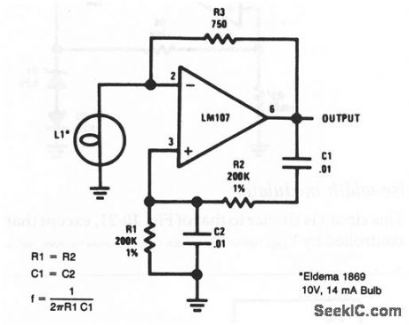
This drcuit is the op-amp version of the dassic Wien-bridge oscillator (chapter 5) using the negative-resistance characteristics of a lamp to stabilize operation. (View)
View full Circuit Diagram | Comments | Reading(1118)
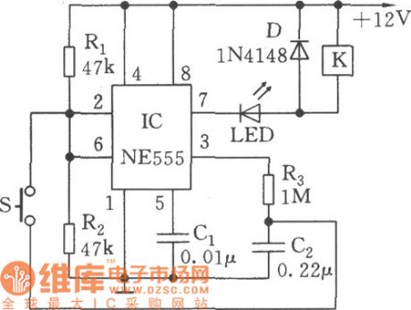
Approach Switch Circuit
Published:2011/7/21 1:41:00 Author:Joyce | Keyword: Approach, Switch
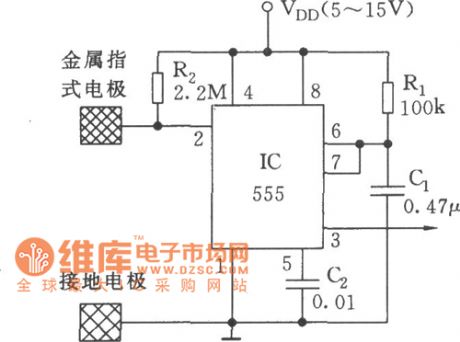
The switch forms a monostable trigger circuit with 555 as the core component .The trigger end feet 2 of is connected with VDD through the major resistance R2, waiting for trigger. When the human body gets close to or touches the metal plate electrode, 555 is activated to output a monostable pulse because of the induction signal. C2 is used to resist interference filter. This circuit can be used for electrical appliances, toys or alarm circuit. (View)
View full Circuit Diagram | Comments | Reading(602)
Multiplexed_cable_driver_2_channel
Published:2009/7/24 21:34:00 Author:Jessie

Figure 6-4 shows a multiplexer/amplifier MAX442 connected to provide 2 channels of video signal to a single cable. Unity-gain bandwidth is 140 MHz, channel-switch time is 36 ns, and slew rate is 250 V/μs. MAXIM NEW RELEASES DATA Book, 1993, P. 3-17. (View)
View full Circuit Diagram | Comments | Reading(588)
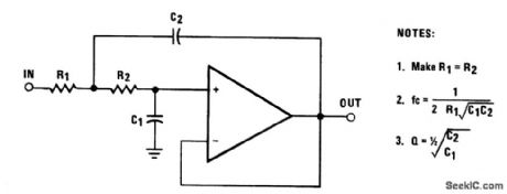
HIGH_Q_BANDPASS_FILTER
Published:2009/6/29 21:41:00 Author:May
View full Circuit Diagram | Comments | Reading(0)
Op_amp_multivibrator
Published:2009/7/24 21:34:00 Author:Jessie
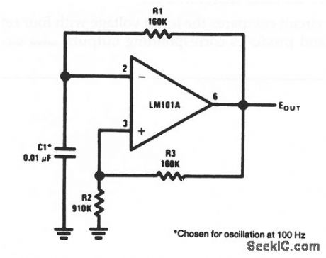
This circuit is the op-amp version of a free-running multivibrator.The square-wave output frequency is set by the value of C1. Notice that both R1 and R3 are 160 kΩ, so that output frequency is directly related to capacitance in μF, using the equation f=1/(6.28 R1C1). (View)
View full Circuit Diagram | Comments | Reading(2555)
| Pages:1240/2234 At 2012211222122312241225122612271228122912301231123212331234123512361237123812391240Under 20 |
Circuit Categories
power supply circuit
Amplifier Circuit
Basic Circuit
LED and Light Circuit
Sensor Circuit
Signal Processing
Electrical Equipment Circuit
Control Circuit
Remote Control Circuit
A/D-D/A Converter Circuit
Audio Circuit
Measuring and Test Circuit
Communication Circuit
Computer-Related Circuit
555 Circuit
Automotive Circuit
Repairing Circuit