
Circuit Diagram
Index 1232
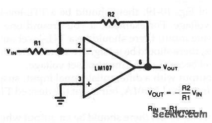
Nonirroerting_amplifier
Published:2009/7/24 20:54:00 Author:Jessie
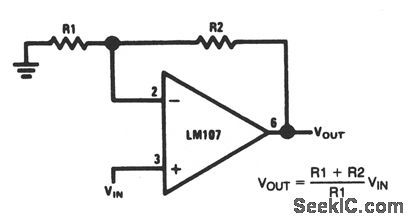
This circuit shows an LM107 in the classic noninverting amplifier configuration, where VOUT follows VIN. The amplitude of the output depends on the ratio of R1 and R2 (within the limits of the supply voltage). The parallel resistance of R1 and R2 should equal the source resistance. (View)
View full Circuit Diagram | Comments | Reading(636)
Common_mode_rejection
Published:2009/7/24 20:40:00 Author:Jessie
There are many definitions for common-mode rejection (CMR), also known as common-mode rejection ratio (CMRR). One definition is the ratio of differential gain (usually large) to common-mode gain (usually a fraction). That is, the amplifier might have a large gain of differential signals (different signals at each input terminal or with one input terminal grounded and the opposite input terminal with a signal), but little gain (or possibly a loss) of common-mode signals (same signal at both terminals). Another definition for CMR is the relationship of change in output voltage to change in input common-mode voltage producing the change, divided by the open-loop gain (amplifier gain without feedback).
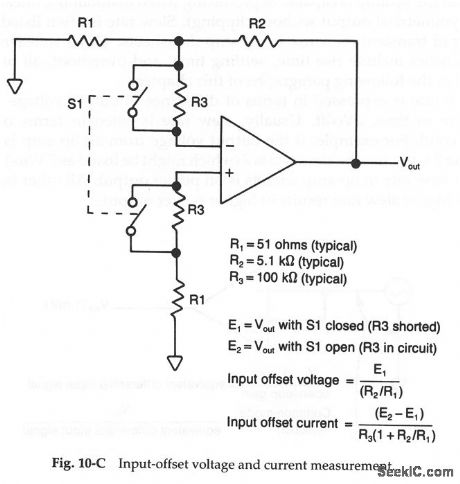
No matter what definition is used, the first step to measure CMR is to find the open-loop gain of the IC at the desired operating frequency (chapter 1). Then, connect the IC in the common-mode circuit of Fig. 10-D. Increase common-mode voltage (at the same frequency used for the open-loop gain test) until a measurable output is obtained. Be careful not to exceed the maximum specified input common-mode voltage swing. If no such value is shown, do not exceed the normal input voltage of the IC. Then, find CMR using the equation.
To simplify the calculation, increase the input voltage until the output is 1 mV. With an open-loop gain of 100, this provides an equivalent differential input signal of 0.00001 V. Then, measure the input voltage. Move the input-voltage decimal point over five places to find CMR. (View)
View full Circuit Diagram | Comments | Reading(973)
DAC_amplifier
Published:2009/7/24 20:40:00 Author:Jessie
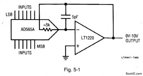
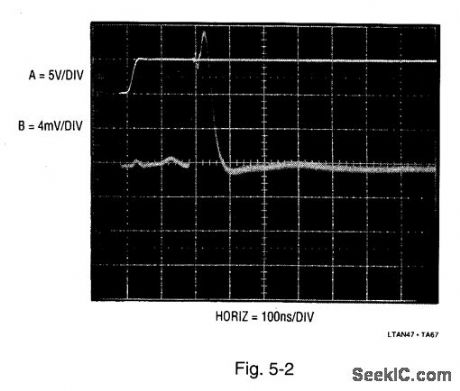
Figure 5-1 shows an amplifier that is suitable for the output of a fast 12-bit DAC (digital-to-analog converter, Chapter 8). Figure 5-2 shows clean 0.01% settling in 280 ns (trace B) to an all-bits-on input step (trace A). LINEAR TECHNOLOGY, APPLICATION NOTE 47, P. 32. (View)
View full Circuit Diagram | Comments | Reading(728)
8038 function generator circuit
Published:2011/7/19 22:19:00 Author:John | Keyword: function generator
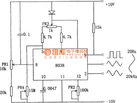
The figure shows the 8038 function generator circuit. Function generator formed by integrated circuit chip 8038 can obtain square wave, triangle wave and sine wave at the same time. Triangle wave can be generated directly by the capacitor discharge current. And square wave can be obtained by control signal. The sine wave is obtained by the broken line approximation circuit from the triangle wave. The sine curve obtained in this way is not a smooth line, whose distortion was about 1 percent. The needs for general purpose can be met. PR1 in the potentiometer circuit is used to adjust the frequency to be ranged from 20 Hz to 20 kHz. PR2 is used to adjust the waveform’s distortion and PR3 is used to adjust the waveform's duty cycle.
(View)
View full Circuit Diagram | Comments | Reading(7881)
Dc_stabilization_with_differential_input_and_a_gain_of_1000
Published:2009/7/24 20:54:00 Author:Jessie
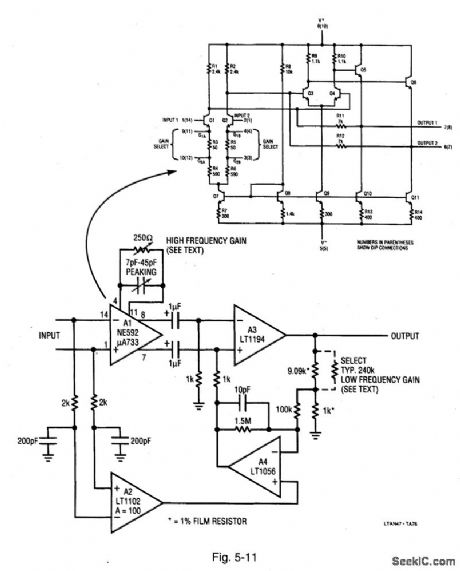
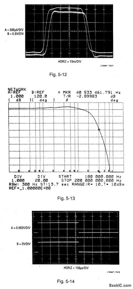
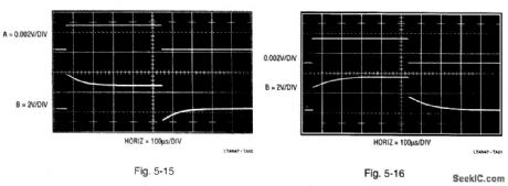
Figure 5-11 is similar to Fig. 5-9, but with a gain of 1000. The Fig. 5-11 circuit bandwidth is about 35 MHz, with full-power response available to 10 MHz. The rise time is 7 ns and delay is less than 7.5 ns. Input noise is about 15 μV broadband.Figure 5-12 shows the circuit response to a 60-ns, 2.5-mV pulse (trace A). The ×1000 output (trace B) has delay and rise times in the 5-ns to 7-ns range. Peaking can be trimmed with the adjustment at A1. Figure 5-13 plots the circuit gain versus frequency. Gain is flat within 0.5 dB to 20 MHz, with the -3-dB point at 38 MHz. The edge peaking shown in Fig. 5-12 shows up in Fig. 5-13 as a very slight gain increase, starting at about 1 MHz and continuing out to about 15 MHz. (This gain increase can be trimmed with the peaking adjustment, if necessary.) To use the circuit, apply a low-frequency or dc signal of known amplitude and adjust the low-frequency gain (parallel resistor) for a ×1000 output (after the output has settled). Next, adjust the high-frequency gain pot so that the output signal front and rear corners have amplitudes identical to the settled portion. Finally, trim the peaking-adjustment capacitor for best settling of the output pulse front and rear corners. Figure 5-14 shows the input (trace A) and output (trace B) waveforms with all adjustments properly set. Figure 5-15 shows the effects of too much ac gain (excessive peaking). figure 5-16 shows the effects of too much dc gain (long trailing response, with incorrect amplitude). LINEAR TECHNOLOGY, APPLICATION NOTE 47, P. 36, 37. (View)
View full Circuit Diagram | Comments | Reading(661)
Inverting_amplifier
Published:2009/7/24 20:53:00 Author:Jessie
This circuit shows an LM107 in the classic inverting-amplifier configuration, where VOUT is opposite to VIN (if VIN goes positive, VOUT goes negative, and vice versa). The amplitude of the output depends on the ratio of R1 and R2 (within the limits of the supply voltage). (View)
View full Circuit Diagram | Comments | Reading(0)
Switch_driver_for_18_V_to_28_V_operation
Published:2009/7/24 20:53:00 Author:Jessie
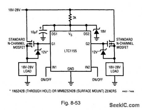
Figure 8-53 shows an LTC1155 connected for 18-V to 28-V switch-driver operation-even though the LTC1154/55/56 family is designed for 4.5-V to 18-V operation. The supply pin (Vs) is clamped to 18 V. These drivers typically produce 36-V of drive from a 18-V supply. This fully enhances N-channel MOSFET switches operating from 18 V to 28 V. The 12-V zener clamps are added to ensure that the maximum MOSFET VGS is not exceeded. LINEAR TECHNOLOGY, APPLICATION Note 53, P.4.
(View)
View full Circuit Diagram | Comments | Reading(702)
CdS photoresistor for electronic metering device circuit
Published:2011/7/28 22:28:00 Author:John | Keyword: CdS photoresistor, electronic metering device
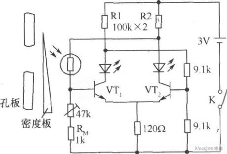
As in block cameras, CdS photoresistor can be used as electronic metering device. The light irradiation passes through the orifice in the CdS photoresistor. The MDF can be moved to achieve a balance of the circuit. When the two LED light emitting diodes are with uniform light, it is said proper to exposure. If only one lights while the other does not, it means that it is with insufficient exposure or over exposure. Thus, the MDF can be moved to achieve the correct exposure. The thermistor RM (1kΩ) in the circuit affects well for temperature compensation and compensates for error caused by temperature change of photosensitive resistor.
(View)
View full Circuit Diagram | Comments | Reading(1876)
Dc_stabilization_with_differential_input_and_gain_of_10
Published:2009/7/24 20:50:00 Author:Jessie

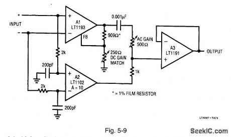
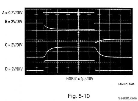
Figure 5-9 shows a way to get full differential inputs with dc-stabilized operation. Figure 5-10 shows the waveforms,Trace A is one side of the differential input applied to the circuit,trace B is the A1 output(taken at the 500-Ω pot and 0.001-μF junction),trace C is the A2 output, and trace D is the A3 output. To adjust, trim the AC GAIN pot for the squarest corners, and the DC GAIN pot for a flat top, of the output signal(trace D).Circuit gain is 10, bandwidth exceeds 35 MHz, slew rate is 450 V/pus, and dc offset is about 200 pV.LINEAR TECHNOLOGY, APPLICATION NOTE 47,P.35. (View)
View full Circuit Diagram | Comments | Reading(729)
Bidirectional_MOSFET_switch_controllers
Published:2009/7/24 20:50:00 Author:Jessie
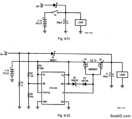
Figures 8-51 and 8-52 show manual and automatic bidirectional switches, respectively. Such circuits are used when the supply voltage is higher or lower than the load voltage, when powered by a secondary source. In the manual circuit of Fig. 8-51, 51 disconnects the battery from both the load and source when VIN (from a wall-unit power supply) is connected. This permits the load voltage to fluctuate above or below the battery voltage, without forcing current into (or out of) the battery. In the far more practical automatic circuit of Fig. 8-52, Q1 and Q2 fully disconnect the battery from the load immediately after the wall-unit supply is connected to VIN. The two diodes in Q1 and Q2 are also connected back to back, and no current can flow through the switch when the gate drive is removed. The LTC1154 EN (enable) input senses when the wall-unit voltage exceeds 3 V, and inverts the switch action so that Q1/Q2 are turned off when the wall-unit supply is disconnected. LINEAR TECHNOLOGY, APPLICATION NOTE 53, P. 3.
(View)
View full Circuit Diagram | Comments | Reading(2068)
Op_amp_troubleshooting
Published:2009/7/24 20:50:00 Author:Jessie
The troubleshooting approach described for the amplifiers of chapter 1 can be applied to op-amp circuits of this chapter. That is, first test the circuit to see if it performs the desired function, If not, try correcting the problem with adjustments. Then, trace signals using a meter or scope from input to output. If any portion of the circuit has a normal input, and an abnormal output, you have located the area in which the trouble occurs. From that point on, it is a matter of voltage measurements and/or point-to-point resistance measurements. The following are a few examples.
In the circuit of Fig. 10-19, there should be a TTL-level output for a small differential input voltage. For example, if you ground one input, and apply a signal to the opposite input, there should be a TTL-level output at pin 6. If you ground both inputs, there should be no signal output. However, the output might shift in voltage level because of the input-offset voltage.
If there is no output with a differential-signal input, suspect the LM101A. If there is an output from the LM101A, but not at the desired TTL level, suspect the LM103.
In the circuit of Fig. 10-20, there should be an output when the photodiode is exposed to light. Because it is difficult to monitor the input current, measure the voltage across R2 (from pin to ground). If there is no change in output voltage when the photodiode is exposed to varying light conditions, suspect the photo-diode, the LM101A, or D2. If the output does change with light current, check the values of R1, R2, and D2. It is also possible that the photodiode is defective, and producing a nonlinear output. (View)
View full Circuit Diagram | Comments | Reading(971)
Dc_stabilization_with_high_input_impedance_
Published:2009/7/24 20:45:00 Author:Jessie
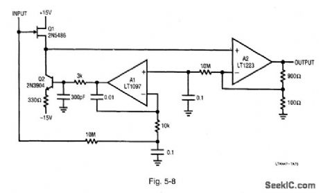
Figure 5-8 shows a dc-stabilized, wideband amplifier using a FET input for high input impedance. Input capacitance is about 3 pF, the bandwidth is 100 MHz, and the gain is 10 (using the feedback values shown). A1 stabilizes the circuit by controlling the Q1 channel current through feedback. LINEAR TECHNOLOGY, APPLICATION NOTE 47, P. 34. (View)
View full Circuit Diagram | Comments | Reading(847)
Dc_stabilization_using_differential_sensing
Published:2009/7/24 20:44:00 Author:Jessie
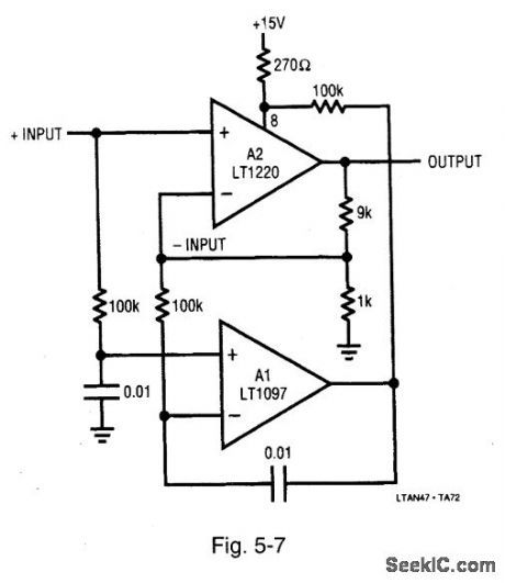
Figure 5-7 is similar to Fig. 5-6, except that the sensing is done differentially, preserving access to both fast amplifier inputs. The combined characteristics of these amplifiers yields the following performance: 50-μV offset voltage, 1-μV/℃ offset drift, 250-V/μs slew rate, and 45-MHz gain bandwidth. LINEAR TECHNOLOGY, APPLICATION NOTE 47, P. 34. (View)
View full Circuit Diagram | Comments | Reading(693)
FOUR_CHANNEL_INPUT_MULTlPLEXING
Published:2009/6/30 1:40:00 Author:May
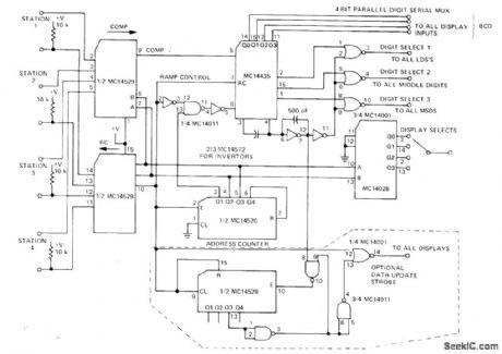
Conversion process is divided between central station and remote locations having analog sensors. Each station transmits two noise-immune low-frequency digital signals under control of central multiplexor. System is much more economical than having separate A/D converter at each sensor. Can be extended to 32 channels. Multiplexing is performed under control of clock in Motorola MC14435, operating between 100 kHz and 1 MHz. At 500 kHz, each conversion takes about 15 ms.—S. Kelley, Analog Data Acquisition Network for Digital Processino Using the MC1405-MC14435 A/D System, Motorola, Phoenix, AZ, 1975, EB-58. (View)
View full Circuit Diagram | Comments | Reading(1235)
SPEECH_FILTER
Published:2009/6/30 1:40:00 Author:May
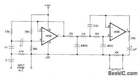
Pair of Bessel-type high-pass filters removes undesired components created by peak clipping during audio signal processing, Developed for use with automatic level control applications of NE571 analog compandor.-W.G. Jung, Gain Control IC for Audio Signal Pro-cessing, Ham Radio, July 1977, p 47-53. (View)
View full Circuit Diagram | Comments | Reading(2359)
TWO_CHANNEL_PANNING
Published:2009/6/30 1:40:00 Author:May
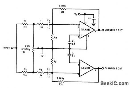
Provides smooth and accurate panoramic control of apparent microphone position between two output channels, as often required in mixing consoles at recording studios, Bequ ires only single linear pot. At each extreme of pot, gain is unity for one channel and zero for other. With pot centered, gains for both channels are -3 dB. R2 depends on supply voltage used, which can be from 9 to 30 V.- Audio Handbook, National Semicon-ductor, Santa Clara, CA, 1977, p 2-59-2-61. (View)
View full Circuit Diagram | Comments | Reading(903)
Dc_stabilization_using_a_summing_point
Published:2009/7/24 20:43:00 Author:Jessie
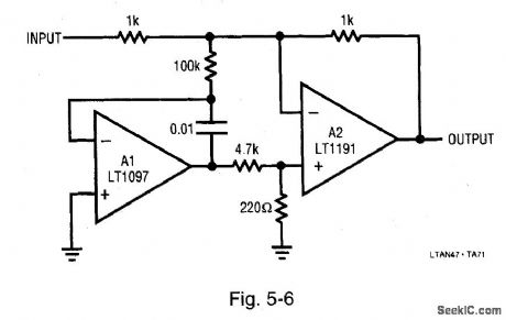
Figure 5-6 shows a circuit where the precision offset of a dc amplifier (LT1097) is combined with the bandwidth of a fast device (LT1191) to provide a dc stabilized, wideband amplifier. The LT1097 monitors the summing node (the two 1-kΩ resistors), compares the node to ground, and drives the LT1191 noninverting input. The resulting circuit is a unity-gain inverter with 35-μV offset, 1.5-V/℃ drift, 450-V/μs slew rate, and 90-MHz bandwidth. Bias current, dominated by the LT1191, is about 500 nA. LINEAR TECHNOLOGY, APPLICATION NOTE 47, P. 33. (View)
View full Circuit Diagram | Comments | Reading(876)
MALE_FEMALE_VOICE_SWITCH
Published:2009/6/30 1:39:00 Author:May
Circuit developed by NASA engineers to improve intelligibility of voice communication during Apollo moon shots passes only the three portions of the speech spectrum required for clear speech:300-400 Hz and 2500-3000 Hz for both sexes and 900-1700Hz for males or t 100-1900 Hz for females. Pot ad lusts null to about 600 Hz. Circuit improves readabilhy of weak DX voice signals in noise.-J. Fisk, Circuits and Techniques, Ham Radio, June 1976, p 48-52. (View)
View full Circuit Diagram | Comments | Reading(845)
WIDEBAND_AF_LEVEL_CONTROL
Published:2009/6/30 1:38:00 Author:May
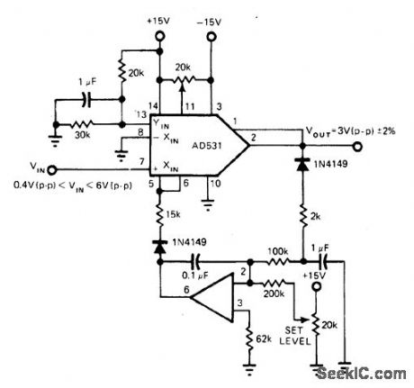
AD531 analog multipliercan hold outputto 3V P-P ±2% for inputs from 0.4 to 6V P-P、at frequencies from 30 Hz to 400 kHz Opamp type is not critical.-R Franlz, Analog Multipliers-New IC Versions Manipulate Real-World Phenomenawith Ease,EDN Magazine, Sept 5、1977,p 125-129. (View)
View full Circuit Diagram | Comments | Reading(638)
Cable_sense_amplifier_for_loop_through_connections
Published:2009/7/24 20:42:00 Author:Jessie
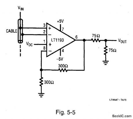
Figure 5-5 shows a differential amplifier used to extract signals from a distribution cable. The amplifier differential inputs reject common-mode signals. Amplifier performance includes 0.02% differential-gain and 0.1° differential-phase errors. A separate input permits dc adjustment. LINEAR TECHNOLOGY, APPLICATION NOTE 47, P. 33. (View)
View full Circuit Diagram | Comments | Reading(640)
| Pages:1232/2234 At 2012211222122312241225122612271228122912301231123212331234123512361237123812391240Under 20 |
Circuit Categories
power supply circuit
Amplifier Circuit
Basic Circuit
LED and Light Circuit
Sensor Circuit
Signal Processing
Electrical Equipment Circuit
Control Circuit
Remote Control Circuit
A/D-D/A Converter Circuit
Audio Circuit
Measuring and Test Circuit
Communication Circuit
Computer-Related Circuit
555 Circuit
Automotive Circuit
Repairing Circuit