
Circuit Diagram
Index 1222
Watchdog_timer_to_prevent_lock_up
Published:2009/7/24 12:39:00 Author:Jessie
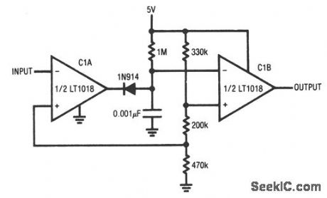
This circuit uses both sections of an LT1018 to prevent lock-up in processor-based systems. Such lock-up can occur if the system misses an instruction because of transients in hardware or software, and usually results in loss of pulses somewhere in the system. This circuit issues a reset command in response to such a pulse loss. Normally, a pulse train appears at the circuit input and causes the C1A output to pulse low. The diode path discharges the 0.01-μF capacitor each time the C1A output goes low. Interruption of the input pulse train (after the 7th vertical division) allows the capacitor to charge beyond the C1B threshold, and triggers C1B low. This pulse can be used to reset the system (applied to the microprocessor RST input). The C1B negative-input RC values can be adjusted to accommodate various input pulse-repetition rates. Linear Technology, Linear Applications Handbook, 1990, p. AN31-10. (View)
View full Circuit Diagram | Comments | Reading(689)
Full_duplex_RS_232_that_uses_negative_charge_storage
Published:2009/7/24 12:36:00 Author:Jessie
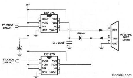
This circuit shows two DS1275 chips to provide full-duplex operation for both TTL and CMOS. Dallas Semiconductors, Product Data Book, 1992/1993, p. 10-113. (View)
View full Circuit Diagram | Comments | Reading(596)
Hand_held_line_powered_RS_232_C_transceiver
Published:2009/7/24 12:34:00 Author:Jessie
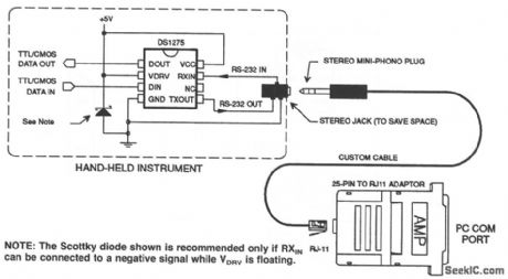
This circuit shows a DS1275 as a hand-held IRS-232-C transceiver using a stereo mini-jack and 25-pin to RK11 adaptor. Notice that the DS1275 accommodates both TTL and CMOS data. Dallas Semiconductors, Product Data Book, 1992/1993, p. 10-113. (View)
View full Circuit Diagram | Comments | Reading(731)
Digital_power_switching_for_SRAMs
Published:2009/7/24 12:29:00 Author:Jessie
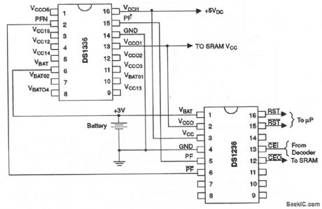
This circuit shows DS1236 and DS1336 chips that are used to provide power switching. When larger operating currents are required in a battery-backed system, the 5-V supply and battery-supply switches within the DS1236 cannot be large enough to support the required load through VCCO with a reasonable voltage drop. When such large currents are required, the PF and PF outputs are provided to gate external power switching devices. Power to the load is switched from VCC to battery on power-down, and from battery to VCC on power-up. The DS1336 uses the PF to switch between VBAT and VCC. The load applied to the PF pin from the extemal switch is supplied by the battery. Thus, if a discrete switch is used, this load should be considered when sizing the battery. Dallas Semiconductors, Product Data Book, 1992/1993, p. 10-77. (View)
View full Circuit Diagram | Comments | Reading(621)
Basic_squaring_circuit
Published:2009/7/24 23:57:00 Author:Jessie
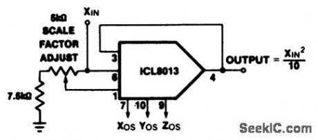
This circuit shows an ICL8013 (refer to Fig. 3-15) connected as a basic ) squaring circuit(with can also be used as the basis for a frequency doubler). (View)
View full Circuit Diagram | Comments | Reading(842)
Bilateral_current_source_with_balance
Published:2009/7/24 21:39:00 Author:Jessie
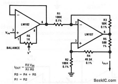
The current output of this circuit depends on the input voltage and the resistance ratios, as shown by the equations. Current output can be trimmed by R6. (View)
View full Circuit Diagram | Comments | Reading(897)
Half_wave_rectifier
Published:2009/7/24 21:38:00 Author:Jessie
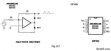
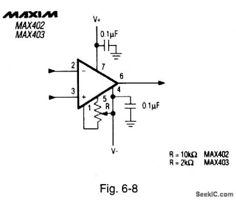
Figure 6-7 shows a MAX402/03 connected to form a half-wave rectifier. The MAX402 has a 5-V/μs slew rate and 1.4-MHz bandwidth with 75 μA for supply current. The MAX403 has a 25-V/μs slew rate and 7-MHz bandwidth, with 375 μA for supply current. Both op amps are unity-gain stable and operate from ±3 V to ±5V, or a single supply from +6 V to +10 V. Figure 6-8 shows a null circuit. MAXIM NEW RELEASES DATA BOOK, 1992, P. 3-15, 3-21. (View)
View full Circuit Diagram | Comments | Reading(0)
Op_amp_pulse_width_modulator
Published:2009/7/24 21:37:00 Author:Jessie
This circuit is similar to that of Fig. 10-21, except that the duty cycle of the output is controlled by VIN. (View)
View full Circuit Diagram | Comments | Reading(735)
Integrator_with_bias_current_compensation
Published:2009/7/24 21:27:00 Author:Jessie
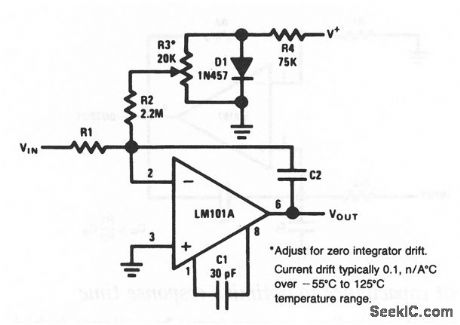
This circuit is similar to that of Fig. 10-10, except that the input bias current can be adjusted for zero drift. (View)
View full Circuit Diagram | Comments | Reading(1694)
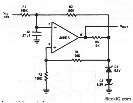
Double_ended_limit_detector
Published:2009/7/24 21:26:00 Author:Jessie
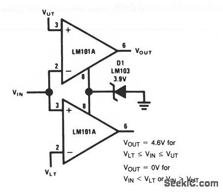
This circuit compares the input voltage with an upper and lower voltage limit. (View)
View full Circuit Diagram | Comments | Reading(2411)
Neutralizing_input_capacitance_to_optimize_response_time
Published:2009/7/24 21:25:00 Author:Jessie
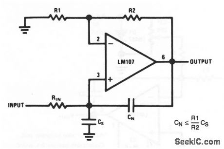
This circuit neutralizes op-amp input capacitance (which tends to restrict circuit response time). (View)
View full Circuit Diagram | Comments | Reading(791)
Positive_voltage_supply
Published:2009/7/24 21:24:00 Author:Jessie
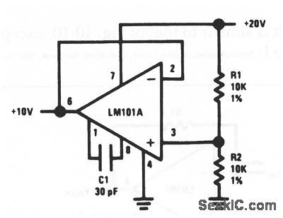
This circuit is designed specifically for the circuit of Fig. 10-13.However, this circuit can be used wherever a +10-V supply is needed. Notice that the output of this circuit is one-half the supply voltage because R1 and R2 are the same value. The same circuit can be used at other supply voltages, and with different ratios of R1 and R2. (View)
View full Circuit Diagram | Comments | Reading(964)
Op_amp_without_a_negative_supply
Published:2009/7/24 21:23:00 Author:Jessie
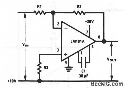
This circuit is similar to that of Fig. 10-2, except that a negative supply is not required. However, a second positive supply (+10 V) is required. The circuit of Fig. 10-14 can be used as the positive supply. (View)
View full Circuit Diagram | Comments | Reading(859)
50_MHz_high_accuracy_analog_multiplier_with_single_ended_output
Published:2009/7/24 21:06:00 Author:Jessie
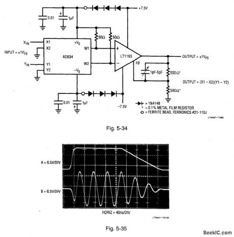
Figure 5-34 shows an analog multiplier with single-ended output. The error is within 2% over the range from dc to 50 MHz, with feedthrough below -50 dB. Figure 5-35 shows the performance when a 20-MHz sine input is multiplied by the trace A waveform, The output (trace B) is a clean instantaneous representation of the X/Y input products, with ±1 V at full scale. To trim, adjust the capacitor for minimum output square-wave peaking. LINEAR TECHNOLOGY, APPLICATION NOTE 47, P. 45. (View)
View full Circuit Diagram | Comments | Reading(757)
40_MHz_fiber_optic_receiver_with_adaptive_trigger
Published:2009/7/24 21:05:00 Author:Jessie
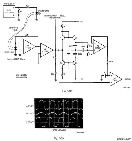
Figure 5-32 shows a circuit that will reliably condition fiber-optic inputs up to 40 MHz with input amplitudes that vary by as much as 40 dB. The digital output features an adaptive threshold trigger which accommodates varying signal intensities. An analog output is also available to monitor the detector output. Figure 5-33 shows the results of using the test circuit in Fig, 5-32. Trace A is the pulse-generator output. Trace B is the A2 output (analog output monitor). Trace C is the LT1016 output. These waveforms were recorded with a 5,ptA photocurrent at about 20 MHz. LINEAR TECHNOLOGY, APPLICATION NOTE 47, P. 44. (View)
View full Circuit Diagram | Comments | Reading(910)
Diode_bridge_based_rectifier_AC_voltmeter
Published:2009/7/24 20:38:00 Author:Jessie
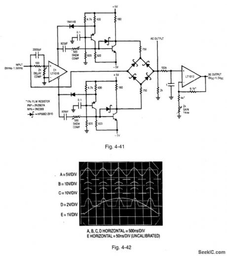
Figure 4-41 shows a circuit that provides both ac and dc outputs for inputs up to 2.5 MHz, Figure 4-42 shows the waveforms. Trace A shows the input sine wave. traces B and C are the switched corners of the bridge, trace D is the ac output, trace E is an expanded version of trace D, To calibrate, apply a 1-MHz to 2-MHz 1-V p-p sine wave and adjust the delay compensation so that bridge switching Occurs when the sine crosses zero. This adjustment corrects for the small delays through the LT1016 and the level shifters. Next, adjust the skew-compensation pots for minimum distortion in the ac output signal(trace D).These trims shift the phase of the rising output edge of their respective level shifter This allows skew in the complementary bridge-drive signals to be kept within 1 ns to 2 ns, minimizing output disturbances when switching Occurs. A 100-mV sine input will produce a clean output with a dc output accuracy of better than 0.25%,LINEAR TECHNOLOGY, APPLICATION Nom 43,P. 34. (View)
View full Circuit Diagram | Comments | Reading(1132)
FOUR_CHANNEL_BCD
Published:2009/6/30 2:56:00 Author:May
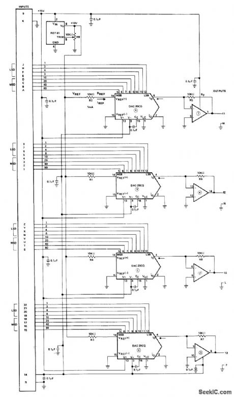
Uses four Precision Monolithics DAC-20CQ 2-digit BCD D/A con verter, OP-11FY precision quad opamp, and REF-01HJ +10 V voltage referenceto convert 2-digit BCD input coding to proportional analog 0 to +10 V output for each of four channels.Same configuration will handle binary inputs, as covered in application note. For output range of 0 to +5 V, change voltage reference to REF-02.—D. Soderquist, Low Cost Four Channel DAC Gives BCD or Binary Coding, Precision Monolithics, Santa Clara, CA, 1977, AN-26, p 3. (View)
View full Circuit Diagram | Comments | Reading(706)
FLASHER_LIGHT_CONTROL
Published:2009/6/30 2:55:00 Author:May
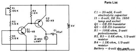
Circuit NotesThe circuit is a two-stage, direct-coupled transistor amplifier connected as a free-running multivibrator. Both the flash duration and flash interval can be changed by turning the potentiometer, R1. (View)
View full Circuit Diagram | Comments | Reading(561)
TONE_CONTROL_CIRCUIT
Published:2009/6/30 2:55:00 Author:May
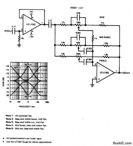
A simple single-transistor circuit will give approximately 15 dB boost or cut at 100 Hz and 15 kHz respectively. A low noise audio type transistor is used, and the output can be fed directly into any existing amplifier volume con-trol to which the tone control is to be fitted. The gain of the circuit is near unity when con-trols are set in the flat position. (View)
View full Circuit Diagram | Comments | Reading(227)
HIGH_SPEED_OUTPUT_OPAMP
Published:2009/6/30 2:55:00 Author:May
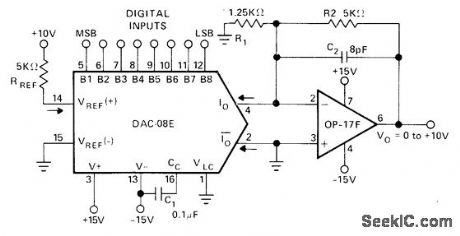
Precision Monolithics OP-17F opamp optimizes DAC-08E D/A converter for highest speed in converting DAC output current to output voltage up to lO V under control of digital input. Settling time is 380 ns.—G. Erdi, The OP-17, OP-16, OP-15 as Output Amplifiers for High Speed D/A Converters, Precision Monolithics, Santa Clara, CA, 1977, AN-24, p 2. (View)
View full Circuit Diagram | Comments | Reading(614)
| Pages:1222/2234 At 2012211222122312241225122612271228122912301231123212331234123512361237123812391240Under 20 |
Circuit Categories
power supply circuit
Amplifier Circuit
Basic Circuit
LED and Light Circuit
Sensor Circuit
Signal Processing
Electrical Equipment Circuit
Control Circuit
Remote Control Circuit
A/D-D/A Converter Circuit
Audio Circuit
Measuring and Test Circuit
Communication Circuit
Computer-Related Circuit
555 Circuit
Automotive Circuit
Repairing Circuit