
Circuit Diagram
Index 1223
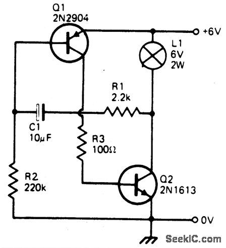
TRANSISTORIZED_FLASHER
Published:2009/6/30 2:55:00 Author:May
Circuit Notes
This simple circuit will flash a 6 volt lamp at a rate determined by the size ofcapacitor C1.It is most economical on power as it only draws current when the lamp is on. When the lamp is off, both transistors are biased off. (View)
View full Circuit Diagram | Comments | Reading(923)
NEON_BLINKER
Published:2009/6/30 2:52:00 Author:May
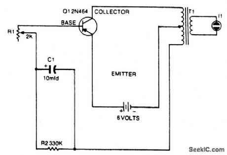
Circuit NotesThe universal output transformer and the transistor form a low-frequency oscillator. The rate of flashing of the neon bulb is determined by potentiometer R1. (View)
View full Circuit Diagram | Comments | Reading(999)
AUTOMATIC_SAFETY_FLASHER
Published:2009/6/30 2:50:00 Author:May
Circuit Notes
This flasher only comes on at night. It furnishes a bright nighttime illumination, and shuts itself off automatically as soon as the sun comes up. The photocell must be mounted on top of the unit in such a way as to detect the greatest amount of available light. (View)
View full Circuit Diagram | Comments | Reading(807)
8_BIT_BINARY_TO_PROCESS_CURRENT
Published:2009/6/30 2:50:00 Author:May
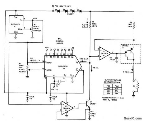
Usesonly three Precision Monolithics ICs operating from -5V and +23 V supplies to convert 8-bit binary digital input to process current in range of 4-20 mA. Fixed current of 0.5 mA is added to DAC output current varying between 0 and 2 mA, with resulting total current multiplied by factor of 8 to give up to 20 mA through 500-ohm load,—D Soderquist, 3 IC 8 Bit Binary Digital to Process Current Converter with 4-20 mA Output, Precision Monolithics, Santa Clara, CA, 1977, AN-21. (View)
View full Circuit Diagram | Comments | Reading(1549)
Basic_crystal_filter
Published:2009/7/24 12:57:00 Author:Jessie
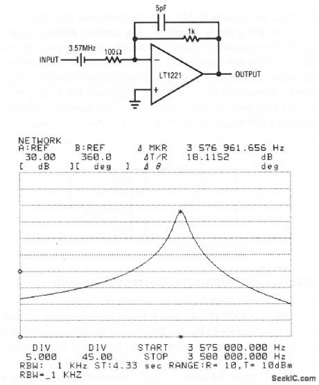
This circuit replaces the ceramic element of Fig. 7-10 with a 3.57-MHz quartz crystal. Figure 7-12B shows almost 30-dB attenuation only a few kHz on either side of resonance. Linear Technology Corporation, 1991, AN47-48/49. (View)
View full Circuit Diagram | Comments | Reading(795)
DUAL_LED_CMOS_FLASHER
Published:2009/6/30 2:49:00 Author:May

Circuit NotesInverters ICl-a and ICl-b form a multivi-brator and IC1-c is a buffer. Inverter IC1-d is connected so that its output is opposite that of ICl-c; when pin 6 is high, then pin 8 is low and vice versa. Because pins 6 and 8 are constantly changing state, first one LED and then the other is on since they are connected in reverse.The light seems to jump back and forth be-tween the LED's. The 470-ohm resistor limits LED current. Depending upon the supply vol-tage used, the value of the resistor may have to be changed to obtain maximum light output. To change the switching rate, change the value of the capacitor. (View)
View full Circuit Diagram | Comments | Reading(1799)
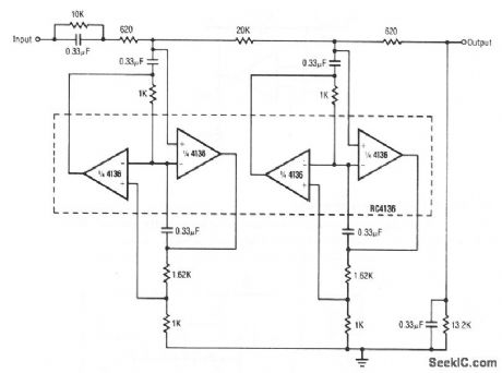
THREE_BAND_ACTIVE_TONE_CONTROL
Published:2009/6/30 2:49:00 Author:May
View full Circuit Diagram | Comments | Reading(0)
Piezo_ceramic_based_filter_with_differential_network
Published:2009/7/24 12:56:00 Author:Jessie
This circuit is an improved version of the Fig. 7-10 circuit. With the Fig. 7-11 circuit, a portion of the input is fed to the noninverting input of A1. The RC network at this input looks like the ceramic-resonantor impedance when it is off null, As a result, A1 sees similar signals for out-of-band inputs. The high-frequency roll-off of Fig. 7-11 is smooth and about 20 dB deeper than the Fig. 7-10 filter at 475 kHz. The low-frequency side of resonance has similar characteristics at 375 kHz and below. Linear Technology Corporation, 1991, AN47-48. (View)
View full Circuit Diagram | Comments | Reading(663)
HI_FI_TONE_CONTROL_CIRCUIT_HIGH_Z_INPUT
Published:2009/6/30 2:48:00 Author:May
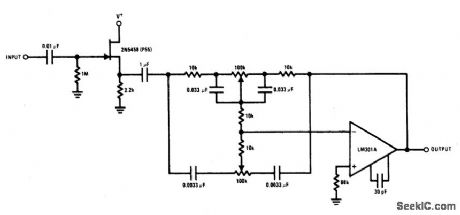
The 2N5458 JFET provides the function of a high input impedance and low noise characteristics to buffer an op amp feedback tone control circuit. (View)
View full Circuit Diagram | Comments | Reading(815)
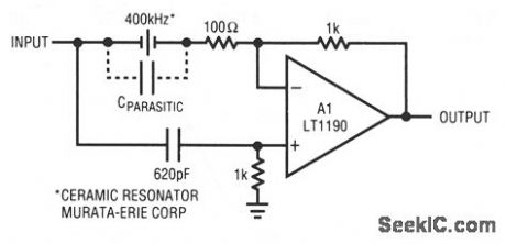
Basic_piezo_ceramic_based_filter
Published:2009/7/24 12:55:00 Author:Jessie
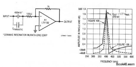
This circuit is a highly selective bandpass filter that uses a resonant ceramic element and a single amplifier. The ceramic element looks like a high impedance off the resonant frequency (400 kHz, in this case). At resonance, the ceramic element has a low impedance, and A1 responds as an inverter with gain. As shown, the ceramic element has stray or parasitic capacitance that causes a slight rise in output at frequencies above 425 kHz. Typically, the A1 output is down about 20 dB at 300 kHz and 40 dB at 425 kHz. The parasitic capacitance can be minimized with a differential network (Fig. 7-11). Linear Technology Corporation, 1991, AN47-48. (View)
View full Circuit Diagram | Comments | Reading(706)
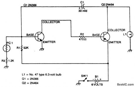
RING_COUNTER_FOR_INCANDESCENT_LAMPS
Published:2009/6/30 2:48:00 Author:May
View full Circuit Diagram | Comments | Reading(963)
Elliptic_filter_
Published:2009/7/24 12:53:00 Author:Jessie
With the values shown, this circuit provides a 4th-order 1-kHz elliptic filter (with 4 poles and 4 zeros). The equations are given for other frequencies. Raytheon Linear integrated Circuits, 1989, p. 4-266. (View)
View full Circuit Diagram | Comments | Reading(2011)
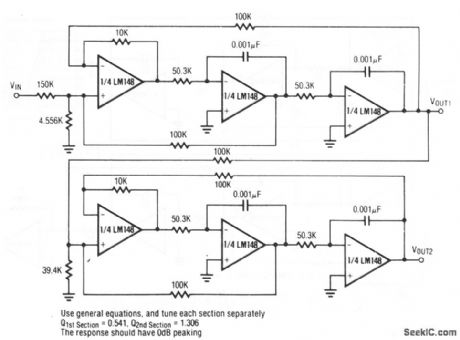
Bi_quad_notch_filter
Published:2009/7/24 12:52:00 Author:Jessie
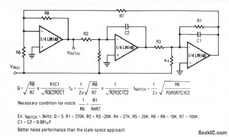
This circuit uses three sections of a quad op amp to form a notch filter. Circuit values are given for a 3-kHz notch with a Q of 5. The equations are given for other frequencies. Raytheon Linear integrated Circuits, 1989, p. 4-266. (View)
View full Circuit Diagram | Comments | Reading(981)
4_pole_Butterworth_filter
Published:2009/7/24 12:51:00 Author:Jessie
With the values shown, this circuit provides a 1-kHz 4-pole Butterworth filter function, with a direct-coupled input and outputs. Raytheon Linear integrated Circuits, 1989, p. 4-265. (View)
View full Circuit Diagram | Comments | Reading(1638)
MICROPHONE_PREAMPLIFIER_WITH_TONE_CONTROL
Published:2009/6/30 2:47:00 Author:May
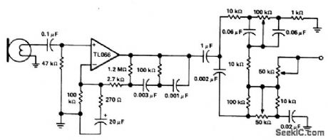
View full Circuit Diagram | Comments | Reading(1259)
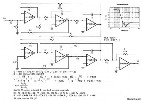
Universal_state_space_filter
Published:2009/7/24 12:50:00 Author:Jessie
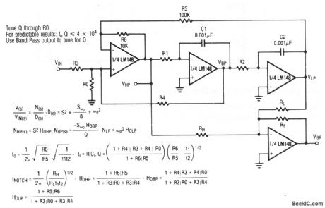
This circuit uses all four sections of a quad op-amp to form a universal state-space filter. Raytheon Linear integrated Circuits, 1989, p. 4-265. (View)
View full Circuit Diagram | Comments | Reading(851)
Dc_coupled_low_pass_active_filter
Published:2009/7/24 12:49:00 Author:Jessie
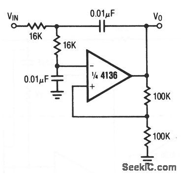
With the values shown, this circuit provides a 1-kHz low-pass filter function, with a direct-coupled input and output. Raytheon Linear integrated Circuits, 1989, p. 4-174. (View)
View full Circuit Diagram | Comments | Reading(790)
Low_pass_Butterworth_active_filter
Published:2009/7/24 12:48:00 Author:Jessie
With the values shown, this circuit provides a 400-Hz low-pass filter function. Raytheon Linear integrated Circuits, 1989, p. 4-172. (View)
View full Circuit Diagram | Comments | Reading(726)
LOW_COST_RING_COUNTER
Published:2009/6/30 2:47:00 Author:May
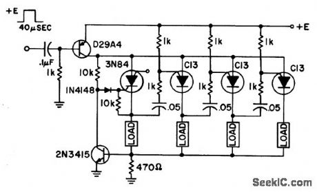
Circuit Notes
This ring counter makes an efficient, low cost circuit featuring automatic resetting via the first stage 3N84. As many stages as desired may be cascaded. (View)
View full Circuit Diagram | Comments | Reading(896)
_15_V_TO__27_V
Published:2009/6/30 2:47:00 Author:May
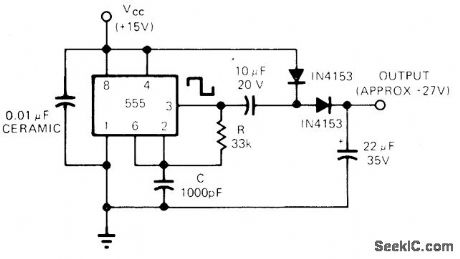
Uses 555 timer in self-triggered mode as square-wave generator operating at about 20 kHz, followed by voltage-doubling rectifier. Provides approximate doubling of voltage without use of transformer. Maximum load current is about 80 mA.—M. Strange, IC Timer Makes Transformerless Power Converter, EDN Magazine, Dec. 20, 1973, p 81. (View)
View full Circuit Diagram | Comments | Reading(2001)
| Pages:1223/2234 At 2012211222122312241225122612271228122912301231123212331234123512361237123812391240Under 20 |
Circuit Categories
power supply circuit
Amplifier Circuit
Basic Circuit
LED and Light Circuit
Sensor Circuit
Signal Processing
Electrical Equipment Circuit
Control Circuit
Remote Control Circuit
A/D-D/A Converter Circuit
Audio Circuit
Measuring and Test Circuit
Communication Circuit
Computer-Related Circuit
555 Circuit
Automotive Circuit
Repairing Circuit