
Circuit Diagram
Index 1224
±15_V_FROM_12_V
Published:2009/6/30 2:46:00 Author:May

Steps up output of 12-V bat-tery to voltages required by PLL such as NE561. Uses 900-Hz sine-wave oscillator and LM380N AF amplifier to drive voicecoil side of standard 500-ohm to 3.2-ohm output transformer having bridge rectifier across center-tapped primary. With 10-mA loads, maximum ripple is 15 mV P-P. With receiver quiet, 900-Hz hum is audible, but is normally lost under background noise. Oscillator choke (about 700 mH) is 800 turns of No. 44 magnet wire in Ferroxcube 30 pot core.—R. Megirian, Build a Noise-Free Power Supply, 73 Magazine, Dec. 1977, p 208-209. (View)
View full Circuit Diagram | Comments | Reading(1291)
Bi_quad_filter
Published:2009/7/24 12:46:00 Author:Jessie
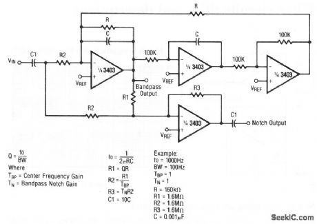
This circuit provides both a notch output and bandpass output. Raytheon Linear integrated Circuits, 1989, p. 4-161. (View)
View full Circuit Diagram | Comments | Reading(889)
LOW_FREQUENCY_LAMP_FLASHER_RELAY_DRIVER
Published:2009/6/30 2:45:00 Author:May
Circuit Notes
This circuit is a low frequency waming device. The output of the oscillator is a square wave that is used to drive lamps or small relays. The circuit altemately flashes two incandescent lamps. (View)
View full Circuit Diagram | Comments | Reading(726)
Multiple_feedback_bandpass_filter
Published:2009/7/24 12:45:00 Author:Jessie

This circuit uses one section of a 3403 op amp with multiple feedback to form a bandpass filter. Raytheon Linear integrated Circuits, 1989, p. 4-160. (View)
View full Circuit Diagram | Comments | Reading(2666)
HIGH_QUALITY_TONE_CONTROL
Published:2009/6/30 2:45:00 Author:May
The circuit is based on an inverting op amp using discrete transistors to overcome poor slew rate, fairly high distortion, and high noise problems. The output stage is driven by a con-stant current source, biased by a green LED to provide temperature compensation. With the controls flat, the unit provides unity gain so the stage can be switched in or out. The design is suitable for inputs between 100 mV and 1 V and provides a good overload margin at low distor-tion for the accurate reproduction of transients. The usual screening precautions against hum should be carried out. (View)
View full Circuit Diagram | Comments | Reading(1245)
Notch_filter_using_an_op_amp_as_a_gyrator
Published:2009/7/24 12:44:00 Author:Jessie
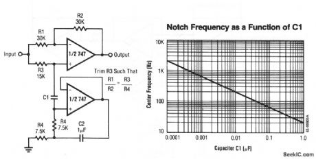
The center or notch frequency of this circuit is determined by the value of C1. Raytheon Linear integrated Circuits, 1989, p. 4-150. (View)
View full Circuit Diagram | Comments | Reading(1026)
_15_V_TO__12_V
Published:2009/6/30 2:44:00 Author:May
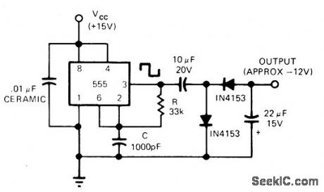
Simple transformerless power converter uses 555 timer in self-triggered mode as square-wave generator, followed by voltage-doubling rectifier. Values shown for R and C give frequency of about 20 kHz, which permits good filtering with relatively small capacitors. Maximum load current is about 80 mA.—M. Strange, IC Timer Makes Transformerless Power Converter, EDN Magazine, Dec. 20, 1973,p 81. (View)
View full Circuit Diagram | Comments | Reading(1726)
FLASHLIGHT_FINDER
Published:2009/6/30 2:44:00 Author:May
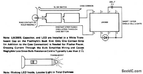
View full Circuit Diagram | Comments | Reading(645)
FLIP_FLOP_FLASHER
Published:2009/6/30 2:43:00 Author:May
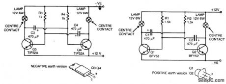
Circuit Notes
The flashing action is provided by a simple astable multivibrator timed to give a flashing rate of about 60 flashes for each lamp per minute. Circuit for positive earth systems uses NPN transistors. The other uses PNP transistors. (View)
View full Circuit Diagram | Comments | Reading(1040)
_12_V_TO_-2_V
Published:2009/6/30 2:42:00 Author:May
High-effkiency polarity inverter for mobile applications provides wellregulated ad justable negative output voltage at 2 A from positive auto battery source. Stable UJT oscillator al drives transistor Q2 to produce symmetrical square wave. Q3 buffers output and furnishes driving power for inverter Q4 and output stage Q7. Q4 and Q5 together drive Q6 into complete saturation. Q6 and Q7 form complementary-symmetry output operating in saturation mode, with only one transistor turned on at a time. As they are alternately switched on and off, square wave alternating between ground and nearly battery potential is applied to Q3. Q10 and Q11 are connected as diodes for clamping square wave negatively. Output voltage is regulated by transistor feedback loop Q8 and Q9, with zener CR2 providing stable reference. R10 is 100 ohms for 2 A maximum; increasing its value improves efficiency but reduces maximum current.—J. R. Laughlin, Medium Current Polarity Inverter, Ham Radio, Nov. 1973, p 26-30. (View)
View full Circuit Diagram | Comments | Reading(1745)
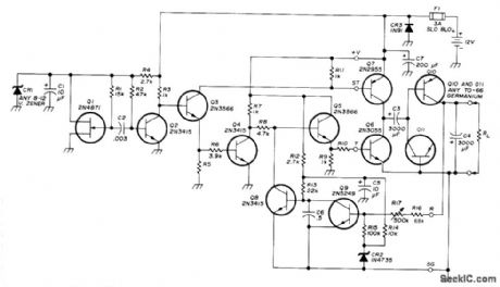
MICROWAVE_DOPPLER_INTRUSION_ALARM
Published:2009/6/30 2:41:00 Author:May
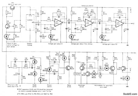
Mullard CL8960 X-band Doppler radar module detects movement of remote target by monitoring Doppler shift in microwave radiation reflected from target. Module consists of Gunn oscillator cavity producing energy to be radiated, mounted alongside mixer cavity that combines reflected energy with sample of oscillator signal. Transmitted frequency is 10.7 GHz. Doppler change is about 31 Hz for relative velocity of 0.45 m/s (1 mph) of relative velocity between object and module, giving AF output for velocities up to 400 mph. Filtered AF is applied through diode pump to trigger of silicon controlled switch TR3 that makes contacts of reed relay open for about 1 s.Relay action is repeated as long as intruder is in monitored area. Report covers circuit operation in detail.-J.E.Saw, Microwave Doppler Intruder Alarms. Mullard, London, 1976, Technical Information 36, TP1570, p 6. (View)
View full Circuit Diagram | Comments | Reading(3588)
AUTO_BOAT_OR_BARRICADE_FLASHER
Published:2009/6/30 2:40:00 Author:May
View full Circuit Diagram | Comments | Reading(698)
LATCHING_ALARM
Published:2009/6/30 2:38:00 Author:May
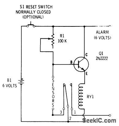
Closed-circuit alarm drawing only 130 μA of standby current from battery is turned on by opening sensor switch or outing wire. Automatic latching contacts on relay prevent burglar or intruder from deactivating alarm by resetting sensor switch, Relay is Radio Shack 275-004. Sensor can be foil strip around window subiect to breakage.-F. M. Mims, Transistor Projects, Vol. 3, Radio Shack, Fort Worth, TX, 1975, p 75-86. (View)
View full Circuit Diagram | Comments | Reading(1723)
Digital level display ( CD40147, CD4511 )
Published:2011/7/19 22:49:00 Author:zj | Keyword: Digital level display
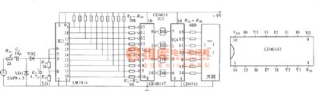
As shown in the figue thedigital level display candisplay audio amplifier output volume levels with digital display. Due to the adoption of a digital display tube,it displays0 ~ 9 levels.
(View)
View full Circuit Diagram | Comments | Reading(2477)
LIGHT_INTERRUPTION_DETECTOR
Published:2009/6/30 2:37:00 Author:May
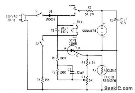
Use of SCR as regenerative amplifier rather than as switch gives extremely high sensitivity to very slight reductions in light reading photoresistor. Requires no light source or accurately aligned light-beam optics. In typical application as burglar alarm, light shining through window from streetlight provides sufficient ambient illumination so any movement of intruder within 10 feet of unitwill energize Sonalertalarm. Sensitivity control R4 is adjusted so SCR receives positive pulses from AC line, but their amplitude is not quite enough to start regenerative action of SCR. Reduction in light then increases resistance of photoresistor enough to raise level of gate pulses for SCR, starting regenerative amplification that energizes relay. Use Mallory SC-628P Sonalert which produces pulsed 2500-Hz sound. With S2 open, alarm stops when changes in light cease. With S2 closed, alarm is latched on and S1 must be opened to stop sound.-R. F. Graf and G. J. Whalen, The Build-It Book of Safety Electronics, Howard W. Sams, Indianapolis, IN, 1976, p 7-12. (View)
View full Circuit Diagram | Comments | Reading(0)
Counting type peak holding circuit(CD4069,CD4081)
Published:2011/7/19 22:58:00 Author:zj | Keyword: Counting type, peak holding circuit
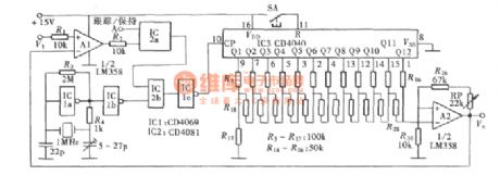
In daily life, we often need to know some physical quantities such as the maximum value, maximum velocity, maximum water level, highest temperature, maximum pressure etc. These physical quantities are usually transmitted to the measuring instrument for measuring through the associated sensor after receiving and transform and display through the instrument. And the instrument always shows the measured value at the time, this value is always changing along with the time.
(View)
View full Circuit Diagram | Comments | Reading(2549)
Simple_low_pass_filter
Published:2009/7/24 13:49:00 Author:Jessie
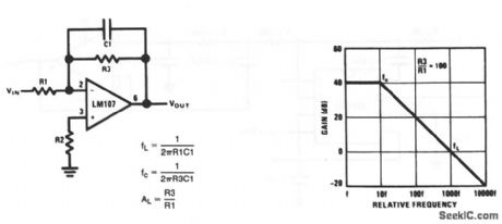
This circuit has a 6-dB per octave rolloff, after a closed-loop 3-dB point that is defined by fc(Fig. 7-41B). Gain below the fc corner frequency is defined by the ratio of R3 to R1. The circuit can be considered as an integrator at frequencies well above fc. However, the time-domain response is that of a single RC, rather than an integral. R2 should be chosen equal to the parallel combination of R1 and R3 to minimize bias-current errors. The op amp should be compensated for unity-gain, or an internally compensated op amp should be used. National Semiconductor, Linear Applications Handbook, 1991, p. 23, 24. (View)
View full Circuit Diagram | Comments | Reading(683)
_12_V_TO__20_V
Published:2009/6/30 2:37:00 Author:May
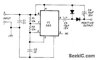
Developed for use with mobile equipment when DC voltage higher than that of auto battery is needed. One application is trickle-charging 12-V nickel-cadmium batteries. Un is 555 timer operated as free-running square-wave oscillator. Frequency is determined by R1, R2, and 02; with values shown, it is about 6 kHz.C1 reduces 6-kHz signal radiated back through input lines. If converter is used with high-frequency receiver, insert 100-μH RF chokes in power leads to suppress harmonics of 6 kHz. For 12-V input, typical outputs are 20.4 V at 10 mA, 19.9 V at 20 mA, and 17.7 V at 50 mA. All diodes are 1N914, 1N4148 or equivalent.—G. A. Graham, Low-Power DC.DC Converter; Ham Radio, March 1975, p 54-56. (View)
View full Circuit Diagram | Comments | Reading(1127)
Dc_accurate_low_pass_Bessel_filter
Published:2009/7/24 13:47:00 Author:Jessie
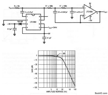
This circuit uses an LTC1050 and LTC1062 to form a low-cost 7th-order 10-Hz low-pass filter, where amplitude and phase response closely approximate a Bessel filter. The required clock frequency is 2 kHz, which yields a clock-to-cutoff frequency ratio of 200:1. Figure 7-40B shows the characteristics. Linear Technology, Linear Appications Handbook, 1990, p. DN9-1, -2. (View)
View full Circuit Diagram | Comments | Reading(1323)
8th_order_Chebyshev_bandpass_filter
Published:2009/7/24 13:46:00 Author:Jessie
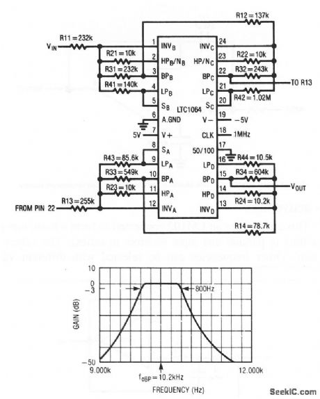
This circuit uses an LTC1064 switched-capacitor filter to form an 8th-order Chebyshev bandpass filter, with a center frequency of 10.2 kHz and a bandwidth of 800 Hz. Figure 7-39B shows the characteristics. Linear Technology, Linear Appications Handbook, 1990, p. AN27A-13, 15. (View)
View full Circuit Diagram | Comments | Reading(1249)
| Pages:1224/2234 At 2012211222122312241225122612271228122912301231123212331234123512361237123812391240Under 20 |
Circuit Categories
power supply circuit
Amplifier Circuit
Basic Circuit
LED and Light Circuit
Sensor Circuit
Signal Processing
Electrical Equipment Circuit
Control Circuit
Remote Control Circuit
A/D-D/A Converter Circuit
Audio Circuit
Measuring and Test Circuit
Communication Circuit
Computer-Related Circuit
555 Circuit
Automotive Circuit
Repairing Circuit