
Circuit Diagram
Index 1234
FET_INPUT_BUFFER
Published:2009/6/30 1:31:00 Author:May
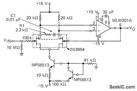
Used ahead of Motorola MC1505 A/D converter to provide input impedance of 10 megohms. FETs are connected as differential amplifier having common source leads returned to constant-current generator built from bipolar transistor, with similar transistor providing temperature compensation. Temperature drift of amplifier is well under 1 mV from 0 to 50℃.—D. Aldridge and S. Kelley, Input Buffer Circuits for the MC1505 Dual Ramp A-to-D Converter Subsystem, Motorola, Phoenix, AZ, 1976, EB-24A. (View)
View full Circuit Diagram | Comments | Reading(999)
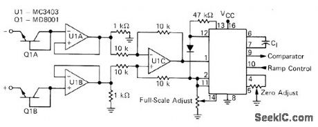
DIFFERENTIAL_OPAMP_AS_BUFFER
Published:2009/6/30 1:30:00 Author:May

Section of Motorola MC3403 quad opamp, operating from single supply, serves as low-cost unity-gain buffer for MC1505 dual-ramp A/D converter. Opamp is used as differential amplifier referenced to MC1505 reference voltage of 1.25 V,—D. Aldridge and S. Kelley, Input Buffer Circuits for the MC1505 Dual Ramp A-to-D Converter Subsystem, Motorola, Phoenix, AZ, 1976, EB-24A. (View)
View full Circuit Diagram | Comments | Reading(990)
CYCLIC_CONVERTER
Published:2009/6/30 1:29:00 Author:May

Unknown voltage is successively compared to reference voltage for determining each digital bit. After determining bit, voltage difference between unknown and reference is operated on, then sent to successive stages to determine less significant bit. Resulting digital output is in Gray-code form. Eight identical circuits are operated in cascade to provide 8-bit A/D converter having accuracy within 1 LSB and full-scale.range of 0-8 V. Circuh requires only two MC1456CG opamps per stage, with MPS6514 transistor as comparator.Switching diode CR1 is MSD6100, and CR2 is MSD6150,Other dioodes are 1N914,—JBarnes, Analog-to-Digitai Cyclic Converter, Motorola, Phoenix, AZ, 1974, AN-557、P 7. (View)
View full Circuit Diagram | Comments | Reading(2188)
HIGH_IMPEDANCE_BUFFER
Published:2009/6/30 1:26:00 Author:May
Two sections of Motorola MC3403 quad opamp serve as voltage followers for differential inputs of third section connected as buffer for MC1505 A/D converter.Dual transistor 01, connected as dual diode, provides 0.6-V offset at inputs of voltage followers, to obtain temperature tracking and predictable performance at low bias currents of opamp.—D. Aldridge and S. Kelley, Input Buffer Circuits for the MC1505 Dual Ramp A-to-D Converter Subsystem, Motorola, Phoenix, AZ, 1976, EB-24A. (View)
View full Circuit Diagram | Comments | Reading(1164)
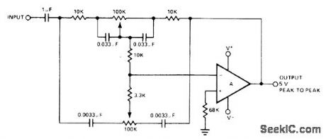
notch filter with easy adjustment circuit
Published:2011/7/28 21:26:00 Author:John | Keyword: notch filter
Notch filter with easy adjustment circuit is shown.
(View)
View full Circuit Diagram | Comments | Reading(668)
0_10_V_ANALOG_INPUT
Published:2009/6/30 1:25:00 Author:May
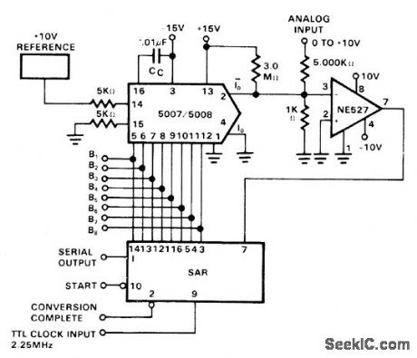
Used to provide digital input to computer for processing and storage of analog signals. Requires only three ICs in addition to external +10 V reference and 2.25-MHz TTL clock. Successive-approximation register (SAR) can be Motorola MC1408 or equivalent. For continuous conversions, connect pins 10 and 2 of SAR.— Signetics Analog Data Manual, Signetics, Sunnyvale, CA, 1977, p 677-685. (View)
View full Circuit Diagram | Comments | Reading(1595)
AUTORANGING
Published:2009/6/30 1:24:00 Author:May
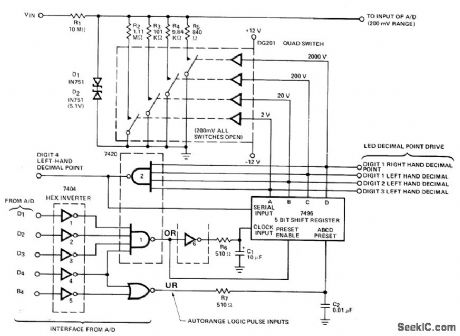
Digitally controlled attenuator uses DG201 quad analog switch as input ladder attenuator switches for A/D converter. Switches are controlled by digital logic that detects overrange and underrange information from A/D converter and closes appropriate attenuator path. Circuit is suitable for Siliconix LD110/111 or LD111/114 A/D converter,— Analog Switches and Their Applications, Siliconix、Santa Clara、CA、1976, p 6-28. (View)
View full Circuit Diagram | Comments | Reading(2334)
Simple and reliable temperature measurement circuit
Published:2011/7/28 21:25:00 Author:John | Keyword: temperature measurement
Any ordinary diode (eg IN4148), in principle, can be used as a fine electronic thermometer’s sensing element with certain precision. When the diode temperature is increased by 1 degree, its forward voltage drop will reduce 2mV.
As shown in the figure, a constant reference voltage is applied to the input end of op-amp A2. A diode and a resistor are applied to the inverting input of op-amp. Therefore, the current flows through the diode and also flows through the resistor. A constant pressure drop should be maintained on the resistor.
(View)
View full Circuit Diagram | Comments | Reading(2347)
AUDIO_FILTERS_FOR_SNR_MEASUREMENT
Published:2009/6/30 Author:May
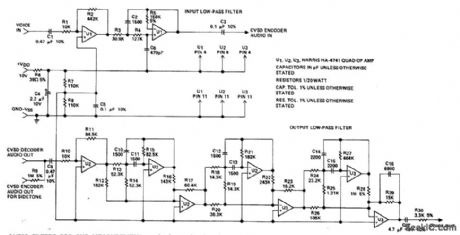
Used in checking performance of Harris HC-55516/55532 haff-duplex modulator-demodulator systems for converting voice signals into s rial NRZ digital data and reconverting that data back to voice. Supply required for opamp sections is ±15 V. Response of input filter is down 3 dB at 3 kHz and is down 20 dB at 9 kHz. Response of output filter is flat up to 3 kHz and down more than 45 dB from 3.8 kHz to 100kHz.- Linear & Data Acquisition Products, Harris Semiconductor,Melbourne,FL,Vol.1,1977,p 5-10. (View)
View full Circuit Diagram | Comments | Reading(746)
COMPRESSOR_1
Published:2009/6/29 23:59:00 Author:May
Keeps output voltage constant as long as input signal is kept above AP threshold level. Opamp is MC3340P. -Circuits, 73 Magazine, Holiday issue 1976, p 170. (View)
View full Circuit Diagram | Comments | Reading(917)
4_μs_CONVERSION_TIME
Published:2009/6/29 23:58:00 Author:May
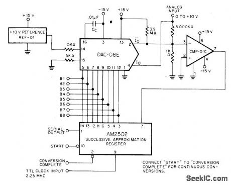
Provides conversion of analog input to 8-bit digital output by suc cessive approximation, with conversion time of 4 μs. Advanced Micro Devices AM2502 successive-approximation register contains logic for Precision Monolithics DAC-08E and CMP-01C comparator.—D. Soderquist and J. Schoeff, Low Cost, High Speed Analog-to-Digital Conversion with the DAC-08, Precision Monolithics, Santa Clara, CA, 1977, AN-16, p 3. (View)
View full Circuit Diagram | Comments | Reading(863)
VOX_WITH_SPEECH_COMPRESSION
Published:2009/6/29 23:58:00 Author:May
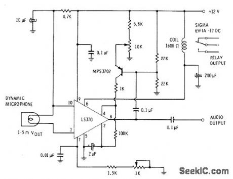
Turns on transmitter automatically when operator begins speaking into microphone. Circuit switches back to receiving condition automatically at end of message. IC can be LS370 or equivalent such as LM370 or SC370. Amount of compression is adjusted with 10K pot, for reducing gain of IC automatically to maintain reasonably constant audio output at pin 8 despite different voice levels at microphone.-E. M.Noll, Linear 10 Principles, Experiments, and Projects, Howard W.Sams,Indianapolis, IN, 1974, p 344-347. (View)
View full Circuit Diagram | Comments | Reading(2549)
8_BIT_SUCCESSlVE_APPROXlMATION
Published:2009/6/29 23:57:00 Author:May
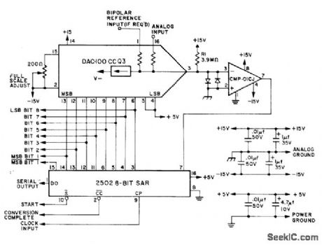
Uses Precision Monolithics DAC-100 CCO3 D/A converter and CMP-01CJ fast precision comparator in combination with Advanced Micro Devices AM2502PC or equivalent successive approximation register to compare analog input with series of trial conversions. Clamp diodes minimize settling time and prevent large inputs from damaging DAC output. Digital output is available in serial nonreturn-to-zero format at data output DO shortly after each positivegoing clock transition.—D. Soderquist, A Low Cost, Easy-to-Build Successive Approximation Analog-to-Digital Converter, Precision Monolithics, Santa Clara, CA, 1976, AN-11, p 3. (View)
View full Circuit Diagram | Comments | Reading(778)
IMPROVED_BAXANDALLCONT_ROL
Published:2009/6/29 23:57:00 Author:May
Uses separate effect″controls for bass and treble tolimit maxlmum degree of boost and cut obtainable from bass and treble controls,R18 controls effect for bass and R21 for treble. Circuit has unity gain with controls set flat. Article gives response curves and describes operation of cir cult in detail-M,V,Thomas、Baxandall ToneControl Revisited、Wireless World, Sept,1974,p341-343. (View)
View full Circuit Diagram | Comments | Reading(2323)
Amplifier circuit of RF2131 with best power and efficiency at 4.0~4.8V power supply
Published:2011/5/6 1:43:00 Author:May | Keyword: Amplifier, 4.0~4.8V power supply, best power and efficiency
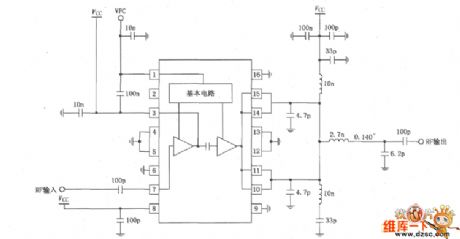
Amplifier circuit of RF2131's best power and efficiency at 4.0~4.8V power supply is shown in the diagram:
(View)
View full Circuit Diagram | Comments | Reading(632)
VIDEO_COMPRESSOR
Published:2009/6/29 23:56:00 Author:May
Nonlinear function amplifier IC-2 compresses video input signals as required to compensate for inefficient quantization where there are too many levels for small signals and too few levels for large signals. Designed to feed 6-bit analog-to-digital converter, IC-1 attenuates input -20 dB and shifts level.Output of IC-2 is amplified by IC-3 to voltage range comparable to that of input signal. IC-4 acts as temperature compensator and output level shifter. R7 nulls small output offsets.—J.B. Frost, Non-Linear Function Amplifier, EEE Magazine, March 1971, p 78. (View)
View full Circuit Diagram | Comments | Reading(728)
SPEECH_FlLTER
Published:2009/6/29 23:56:00 Author:May
High-pass and low pass filters in cascade provide comer frequencies of 300 and 3000 Hz for limiting audio bandwidth to speech frequencies. Rolloff beyond corners is -40 dB per decade. Input-to-output gain is 1.- Audio Handbook, National Semiconductor, Santa Clara, CA, 1977, p 2-49-2-52. (View)
View full Circuit Diagram | Comments | Reading(1263)
10_BIT_ACCURACY
Published:2009/6/29 23:55:00 Author:May
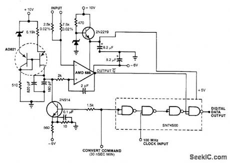
Single-slope A/D converter gives high-speed conversion of DC input voltage to digital data output. For 0-10 V input, 1024 pulses of 100-MHz clock appear at full scale and 512 at half scale. When command pulse is applied, 2N914 transistor resets 1000-pF capacitor (820 and 180 in parallel) to 0 V. Capacitor begins to charge linearly on falling edge of command pulse, to 2.5 V. 10-μs ramp is applied to AMD686 for comparison with unknown voltage. Output of opamp is pulse whose width is proportional to input voltage and can therefore be used to gate 100-MHz clock.—J. Williams, Low-Cost, Linear A/D Conversion Uses SingleSlope Techniques, EDN Magazine, Aug. 5, 1978, p 101-104. (View)
View full Circuit Diagram | Comments | Reading(1117)
TONE_CONTROL_FOR_OPAMP
Published:2009/6/29 23:55:00 Author:May
Provides up to 20 dB of bass boost or cut at 20 Hz and up to 19dB of treble boost or cut at 20 kHz. Turnover fre-quency is 1 kHz. Opamp can be 531 or 301.- Signetics Analog Data Manual, Sunnyvale, CA, 1977, p 638-640. (View)
View full Circuit Diagram | Comments | Reading(1917)
LOW_ON_LOGIC_CONTROL
Published:2009/6/29 23:53:00 Author:May
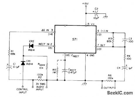
Uses Signetics NE571 or NE570 analog compandor. Gain is determined by current developed through RGAIN in conjunction with intemal 1.8-V voltage reference. When control input is low, normal current flowsthrough RGAIN When control signal is high, CR1 is forward-biased, interrupting current flow, and output is attenuated.-W. G. Jung, Gain Control IC for Audio Signal Processing, Ham Radio, July 1977, p 47-53. (View)
View full Circuit Diagram | Comments | Reading(1056)
| Pages:1234/2234 At 2012211222122312241225122612271228122912301231123212331234123512361237123812391240Under 20 |
Circuit Categories
power supply circuit
Amplifier Circuit
Basic Circuit
LED and Light Circuit
Sensor Circuit
Signal Processing
Electrical Equipment Circuit
Control Circuit
Remote Control Circuit
A/D-D/A Converter Circuit
Audio Circuit
Measuring and Test Circuit
Communication Circuit
Computer-Related Circuit
555 Circuit
Automotive Circuit
Repairing Circuit