
Circuit Diagram
Index 1233
bridge photoelectric detector composed of photosensitive resistor circuit
Published:2011/7/28 21:53:00 Author:John | Keyword: photosensitive resistor, bridge photoelectric detector
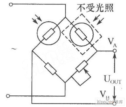
In the industrial optical measuring devices, the photosensitive resistor can be used to form the bridge photoelectric detector, just as shown in the figure. The two same models (with equivalent dark resistance) of the photoresistor are used as the bridge. One is for optical detection and the other is sealed with black tape. It is important to prevent it from being subjected to light as it is for temperature compensation. This type of bridge photodetector can be powered by DC or AC. When AC modulation, is used, its output is the AC signal, thus being able to reduce zero drift for the amplifier.
(View)
View full Circuit Diagram | Comments | Reading(1279)
Simple_video_amplifier
Published:2009/7/24 20:41:00 Author:Jessie
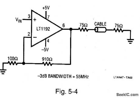
Figure 5-4 is a simpler version of Fig. 5-3, but with only one video channel. The bandwidth of 55 MHz. LINEAR values provide for a gain of 10, with a TECHNOLOGY, APPLICATION NOTE 47, P. 33. (View)
View full Circuit Diagram | Comments | Reading(0)
ALARM_DETECTOR
Published:2009/6/30 1:38:00 Author:May
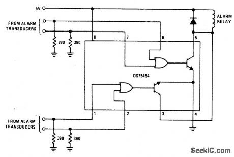
National DS75454 dual peripheral NOR driver operating from single 5-V supply energizes alarm relay when one of alarm transducers for either section delivers logic signal as result of intruder action.- Interface Databook, National Semiconductor, Santa Clara, CA, 1978, p 3-20-3-30. (View)
View full Circuit Diagram | Comments | Reading(664)
Two_channel_video_amplifier
Published:2009/7/24 20:41:00 Author:Jessie
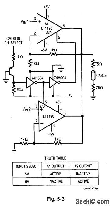
Figure 5-3 shows a simple way to multiplex two video amplifiers onto a single 75-Ω cable. The appropriate amplifier is activated in accordance with the truth table. Amplifier performance includes 0.02% differential-gain and 0.1°differential-phase errors. The 75-Ω back termination looking into the cable means that the amplitude must swing 2 Vp-p to produce 1-Vp-p at the cable output. LINEAR TECHNOLOGY, APPLICATION NOTE 47, P. 33. (View)
View full Circuit Diagram | Comments | Reading(763)
BINARY_OUTPUT
Published:2009/6/30 1:38:00 Author:May
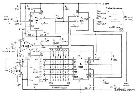
Converts analog signal in range of 0-10 V to 8-bit binary word having all 0s for 0V and all 1s for full-scale input of +9.960V output is 15-V CMOS-compatible but can be adapted for TTL compatibility,Maximum conversion time is about 26 ms. A2 and A3 form negative-going staircase generatof for which startconversion signal is formed by one section of 556. Opamp A4 compares negative output of 7530 with input voltage Vin. When 7530 output voltage equals input voltage, comparator output goes positive and resets control flip-flop to complete gonversion.—W. G. Jung, IC Timer Cookbook, Howard W. Sams, Indianapolis, IN,1977, p 226-228. (View)
View full Circuit Diagram | Comments | Reading(812)
SYMMETRICAL_ACTIVE_CROSSOVER
Published:2009/6/30 1:38:00 Author:May
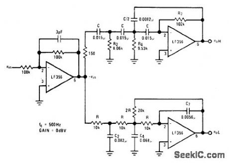
Provides -18dB per octave rolloff (third order) and maximally fiat (Butterworth) characteristics for crossover frequency of 500 Hz. Uses National LF356 opamps in highpass and low-pass filters and same opamp as buffer having low driving impedance required by active filters. Power supplies are ±15V. Design equations are given.- Audio Handbook, National Semiconductor, Santa Clara, CA, 1977, p 5-1-5-7. (View)
View full Circuit Diagram | Comments | Reading(1806)
THUMPLESS_CONTROL
Published:2009/6/30 1:38:00 Author:May
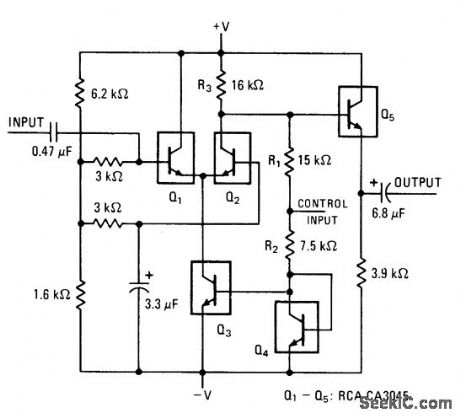
Five-transistor circuit for audio amplifier applications eliminates thumping sounds that can sometimes be heard when Ievel of input signal changes suddenly.Differential amplifier Q1-Q2, with B, in emitter-current control circuit, eliminates thump. Control input acts on identical transistors Q3-Q4 which make transconductance of differential pair Q1-Q2 vary in direct proportion to control voltage. Fifth transistor in array, Q5, is used as outputsignal buffer. Amplifiergain is 30 for control voltage of 15 V.-P. Brokaw, Automatic Gain Control Quells Amplifier Thump, Electron-ics, Jan. 10, 1974, p 131-132; reprinted in Circuits for Electronics Engineers, Electronics, 1977, p 46-47. (View)
View full Circuit Diagram | Comments | Reading(823)
ALARM_SIGNAL_DETECTOR
Published:2009/6/30 1:37:00 Author:May
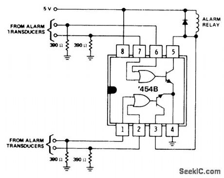
Texas Instruments SN75454B dual peripheral positive-NOR driver energizes alarm relay when alarm signal is received from any one of four different alarm transducers.- The Linear and Interface Circuits Data Book for Design Engineers, Texas Instruments, Dallas, TX, 1973, p 10-66. (View)
View full Circuit Diagram | Comments | Reading(779)
using light-emitting diode for piezoelectric signal generator display circuit
Published:2011/7/28 21:47:00 Author:John | Keyword: light-emitting diode, piezoelectric signal generator
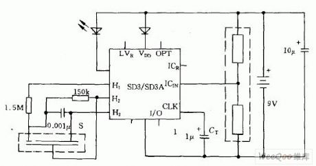
The figure shows the integrated circuit of converting pressure to electrical signal and being sent to SD3 or SD3A followed through the piezoelectric element sensor circuit S. And the signal is displayed through the light-emitting diode. The two equivalent resistors inside of the dashed border of the figure are studio and compensation room respectively (double chamber).
(View)
View full Circuit Diagram | Comments | Reading(1412)
SOUND_OPERATED_RELAY
Published:2009/6/30 1:36:00 Author:May
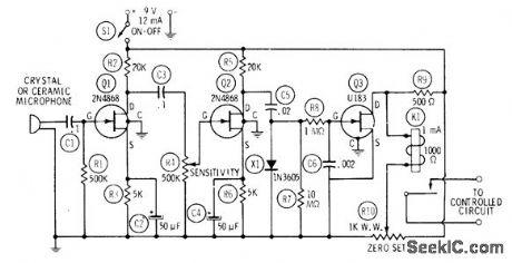
Output of about 1.8 m VRMS from crystal orceramic microphone will energize relay when sensitivity control R4 is at maximum. First two stages form high-gain RC-coupled AF amplifier, output of which is rec-tified by silicon diode X1. DC voltage developed across diode is applied to gate of Siliconix U183 FETwhich acts as DC amplifier driving Sigma 5F or equivalent relay. To ad just, short microphone terminals, set R4 for maximum sensitivity, then ad just R10 until relay opens.-R. P Turner, FET Circuits, Howard W. Sams, Indianapolis, IN, 1977, 2nd Ed., p 111-113. (View)
View full Circuit Diagram | Comments | Reading(1125)
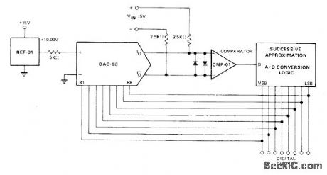
FOUR_QUADRANT_RATIOMETRIC
Published:2009/6/30 1:36:00 Author:May
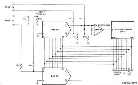


Uses Precision Monolithics DAC-08 D/A converters and CMP-01 comparator to drive successive-approximation conversion logic using REF-01 +10 V reference and 2502-type successive-approximation register. Imputs VX are connected conventionally, and inputs VY are connected in multiplying fashion. IREF for both DACs is modulated between 1 and 3 mA. Resulting output currents are differentially transformed into voltages by 5K resistors at comparator inputs and compared with VX differential input. When conversion process is complete (comparator inputs differentially nulled to less than 1/2 LSB), digital output corresponds to quotient VX/VY. Diodes are 1N4148.—J. Schoeff and D. Soderquist, Differential and Multiplying Digital to Analog Converter Applications, Precision Monolithics, Santa Clara, CA, 1976, AN-19, p 5. (View)
View full Circuit Diagram | Comments | Reading(1575)
AURAL_INDICATOR
Published:2009/6/30 1:36:00 Author:May
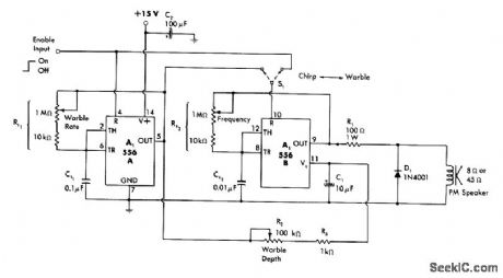
Provides attention-getting chirp sound, warble, or continuous tone when turned on by high input from burglaralarm sensor circuit. Second section of 556 timer provides optional frequency modulation of basic tone to give warbling effect. Chirp is achieved by gating tone oscillator on only during high states of warble oscillator. Aural sensitivity is maximum in range of 1-2 kHz, set by value of Rt2.-W. G. Jung, IC Timer Cookbook, Howard W. Sams, Indianapolis, IN, 1977, p 232-235. (View)
View full Circuit Diagram | Comments | Reading(841)
ENTRY_DELAY_ALARM
Published:2009/6/30 1:35:00 Author:May
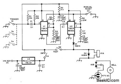
First 555 timer provides delay of about 20 s after triggering by sensor before alarm bell is energized, to allow thief to be caught inside house or give owner time to enter and shut off alarm. Alarm then rings for about 60 s under control of timer U2. Alarm period was set short to attract attention without unduly annoying neighbors.-J. D. Arnold, A Low-Cost Burglar Alarm for Home or Car, QST, June 1978, p 35-36. (View)
View full Circuit Diagram | Comments | Reading(942)
REPETITIVE_MODE_OPERATION
Published:2009/6/30 1:35:00 Author:May
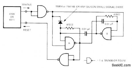
Quicker conversion is obtained in Teledyne Philbrick 4109 or 4111 A/D converter by restarting converter within a few microseconds after status signal, using surestart circuit shown. Reset pulse is fed to converter when status signal is held at low DC level. When status command is high, oscillator A-B is disabled. If reset pulse is not obeyed and status signal remains low, oscillator starts up until conversion does occur.—R.W. Jacobs, Repetitive Mode Operation for Models 4109/4111 Integrating A/D Converters, Teledyne Philbrick, Dedham, MA 1977, AN-28. (View)
View full Circuit Diagram | Comments | Reading(690)
500 candela flash circuit
Published:2011/7/28 21:33:00 Author:John | Keyword: flash, 500 candela flash
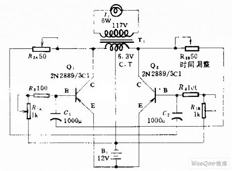
This circuit can be used at night as the flash for dock instruction or rescue vehicle. The flash can be D26-type or 6S6 type of 117V and 6W. Q1 and Q2 form an oscillator alter battery’s direct current into alternating current. The AC can be used as boost power supply for T1. Double potentiometer R2 adjusts the duration of each flash and R1 adjusts the flash frequency.
(View)
View full Circuit Diagram | Comments | Reading(582)
SCR_LATCH
Published:2009/6/30 1:34:00 Author:May
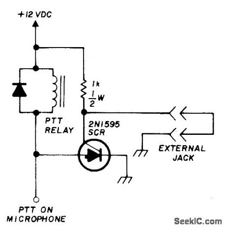
Turns on mobile transceiver or other mobile equipmentwhen powerisapplied, if external circuit is broken when equipment is stolen. Transmitter will then put unmodulated carrier on air even with PTT switch disconnected or off, for tracing with radio direction finder. If added components are carefully concealed in equipment and new external wiring is worked into existing wiring harness, few thieves will be able to locate trouble. External wires are run under dash so thief must cut them to get out equipment. PTT relay should have protective diode. SCR is 100 PIV, 1 A, but HEP R1003 or R1217 can also be used.-E. Noll, Circuits and Techniques, Ham Radio, April 1976, p 40-43. (View)
View full Circuit Diagram | Comments | Reading(2177)
DIFFERENTIAL_CONVERSION
Published:2009/6/30 1:34:00 Author:May
Uses high current output capability of Precision Monolithics DAC-08 D/A converter and high common-mode voltage rejection of CMP-01 comparator to give differential-input ADC without input signal conditioning. Successive-approximation conversion logic is obtained with REF.01 +10 V reference and 2502-type successive-approximat ion register, driven by DAC and comparator. Analog input is converted in less than 2 μs. Differential input range is 5 V. Diodes are 1N4148.—J. Schoeff and D. Soderquist, Differential and Multiplying Digital to Analog Converter Applications, Precision MonolithIcs, Santa Clara, CA, 1976, AN-19, p 5. (View)
View full Circuit Diagram | Comments | Reading(1718)
TRACKING_A_D_CONVERTER
Published:2009/6/30 1:33:00 Author:May
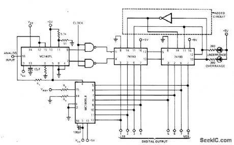
Addition of one gate to tracking or servorype A/D converter, as shown in dashed box, overcomes instability problems otherwise occurring when input voltages are less than zero or greater than full scale. With 8-bit converter shown, count of 11111111 when counting up makes carry output and load inputs go low, holding counter in this state so subsequent up clocks are ignored. When count is all 0s, borrow output goes low and clear input goes high, so counter isfree to countup only.—A. Helfrick, Tracking A/D Converters Need Another Look, EDN Magazine, June 20, 1975, p 118 and 120. (View)
View full Circuit Diagram | Comments | Reading(1560)
FIVE_INDICATOR_ALARM
Published:2009/6/30 1:32:00 Author:May
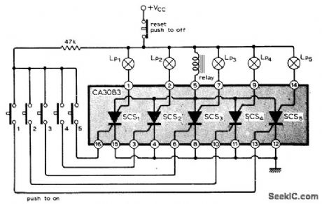
Single five-transistor 10 uses NPN structures on P-type substrate as PNPN silicon controlled switches having common connection for anode (substrate).Relay serving as anode load is energized for actuating alarm if any of the SCS pushbutton switches is closed. Corresponding lamp is energized to identify door or window at which sensor switch has been closed by act of intruder. Alarm remains on until reset by interrupting power supply. Power drain on standby is negligible because SCSs act as open circuits until triggered, permtitting use of batteries for supply. Two or more ICs may be added to get more channels.-H. S. Kothari, Alarm System with Position Indication, Wireless World, Feb. 1976, p 77. (View)
View full Circuit Diagram | Comments | Reading(1040)
Anti-Chi generator circuit
Published:2011/7/28 21:27:00 Author:John | Keyword: generator
Anti-Chi generator circuit is shown.
(View)
View full Circuit Diagram | Comments | Reading(1467)
| Pages:1233/2234 At 2012211222122312241225122612271228122912301231123212331234123512361237123812391240Under 20 |
Circuit Categories
power supply circuit
Amplifier Circuit
Basic Circuit
LED and Light Circuit
Sensor Circuit
Signal Processing
Electrical Equipment Circuit
Control Circuit
Remote Control Circuit
A/D-D/A Converter Circuit
Audio Circuit
Measuring and Test Circuit
Communication Circuit
Computer-Related Circuit
555 Circuit
Automotive Circuit
Repairing Circuit