
Circuit Diagram
Index 1235
HIGH_ON_LOGIC_CONTROL
Published:2009/6/29 23:52:00 Author:May
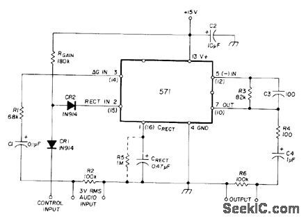
Uses Signetics NE571 or NE570 analog compandor. When control tnput is high, CR1 is off and current developed by RGAIN flows into rectifier input, allowing audio to be amplified. Gain is unity (or other nominal value chosen by changing value of R3) for control inputs greater than 3 V. Switching is abrupt, with full attenuation below 1.5 V. Narrow transition width and nominal DC center of 1.8 V allow direct control from CMOS, rrL, DTL, or other positive logic. Supply voltage should be stable.-W. G. Jung, Gqin Control IC for Audio Signal Processing, Ham Radio, July 1977, p47-53. (View)
View full Circuit Diagram | Comments | Reading(1180)
BASS_TREBLE_BOOST_CUT
Published:2009/6/29 23:52:00 Author:May

Using linear and log pots with tone control network in feedback path of CA3140 bipolar MOS opamp, circuit provides 20-dB gain in flat position and ±15dB bass and treble boost and cut at 100 and 10,000 Hz.Output is 25 V P-P at 20 kHz and is -3 dB at 24 kHz from 1-kHz reference. Optional connection for ±15V supply is also shown.- Circuit Ideas for RCA Linear ICs, RCA Solid State Division, Somerville, NJ, 1977, p 10. (View)
View full Circuit Diagram | Comments | Reading(2285)
ASYMMETRICAL_ACTIVE_CROSSOVER
Published:2009/6/29 23:51:00 Author:May
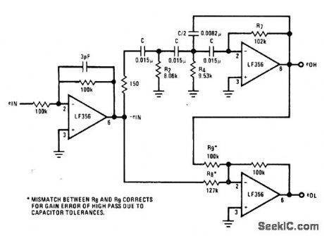
High-pass and low-pass active filters using National LF356 opamps are asymmetrical about 500-Hz crossover point,Sum of filter output voltages is always constant and equaltounity,Rolloff of low-pass filter is only-6 dB peroctave、as compared to-18 dB per octave for high-pass filter,-″Audio Handbook″ National semiconductor, Santa Clara,GA,1977、p 5-1-5-7. (View)
View full Circuit Diagram | Comments | Reading(1877)
CONSTANT_18_V_AF_FOR_SSB
Published:2009/6/29 23:50:00 Author:May
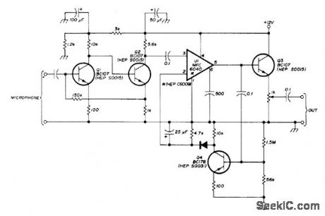
Uses Motorola MFC6040 voltage-controlled amplifierIC having 13-dB gain.and maximum of 90-dB gain reduction. Q1-Q2 form microphone preamp, Q4 is AGC detector/amplifier for IC, and a3 is output buffer. With 500-ohm dynamic microphone, output remains constant at 1.8 VRMS.-L. No-votny, Speech Compressor, Ham Radio, Feb.1976, p 70-71. (View)
View full Circuit Diagram | Comments | Reading(2503)
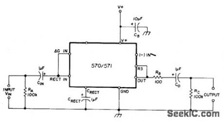
COMPRESSOR
Published:2009/6/29 23:49:00 Author:May
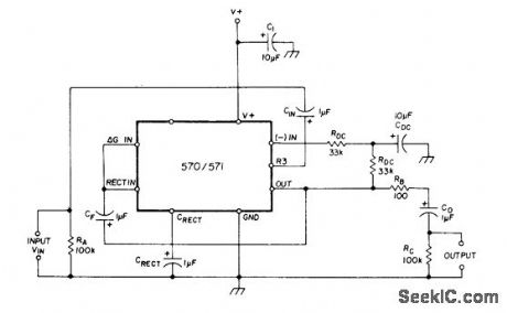
Circuit has unity gain at 0.775 VRMS input and complementary input/output characteristic. Voltage gain through compres sor is square root of 0.7/VIN where VIN is avefage input voltage. Uses Signetics dualchannel compandor IC; 571 has lower inherent distortion and higher supply voltage range (6-24 V) than 571 (6-18 V).-W. G. Jung, Gain Control IC for Audio Signal Processing, Ham Radio, July 1977, p 47-53. (View)
View full Circuit Diagram | Comments | Reading(5482)
ROOM_E0UALIZER
Published:2009/6/29 23:48:00 Author:May
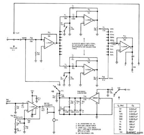
Ten-octave equalizer is combined with pink-noise generator in such away that all but one octave band can be switiched out,Mith pink noise passed through remaining filter to power amplifier and loudspeaker,Microphone with flat frequency response over audio band is used to pick up resulting noise at some center listening point in room being equalized. Ampllfied output ot microphone drives VU meter where arbitrary level is established for one filter section. Other filter sections are then switched in one at a time and adjusted to give same VU reading. Equalizer settings then give flat room response for all ten octaves. High end can then be rolled off or low end boosted to suit personal preference. Adjustments are readily repeated when fumiture is changed in room. Table gives values of C1 for each octave.- Audio Handbook, National Semiconductor, Santa Clara, CA, 1977, p 2-53.-2-59. (View)
View full Circuit Diagram | Comments | Reading(1198)
AF_LEVEL_CONTROL
Published:2009/6/29 23:47:00 Author:May
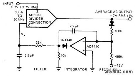
AD533J analog multiplier used in its divide mode provides measure of automatic level control to compensate for variations in loudness occurring from micro-phone to microphone in publicaddress system.Divider output is first rectified and compared with -15 V reference, Difference is then integrated and fed into denominator of divider-connected AD533J as control signal Vx. Average AC output is held within 1% of 7 V.-R. Frantz, An-alog Multipliers-New IC Versions Manipulate Real-World Phenomena with Ease, EDN Magazine, Sept. 5, 1977, p 125-129. (View)
View full Circuit Diagram | Comments | Reading(828)
Basic_division_circuit
Published:2009/7/24 23:57:00 Author:Jessie
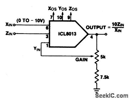
This circuit shows an ICL8013 (refer to Fig. 3-15) connected as a basic divider. Use the following trim procedure.1. Set the trim pots (Fig. 3-15D) at mid-scale by adjusting the voltage on pins 7, 9, and 10 for 0 V.2. With ZIN= 0V, trim Z0s to hold the output constant as XIN is varied from -10 V through -1 V.3. With ZIN= 0 V and XIN =10.0 V adjust Yos for zero output voltage.4. With ZIN=XIN (and/or ZIN =-XIN) adjust Xos for minimum worst-case variation of output as XIN is varied from -10 V to -1 V.5. Repeat steps 2 and 3 if step 4 requires a large initial adjustment.6. With ZIN = XIN (and/or ZIN = -XIN), adjust the gain control until the output is the closest average around +10.0 V (-10 V for ZIN =-XIN) as XIN is varied from -10 V to-3 V. (View)
View full Circuit Diagram | Comments | Reading(744)
OTA_single_control_function_generator
Published:2009/7/24 23:54:00 Author:Jessie
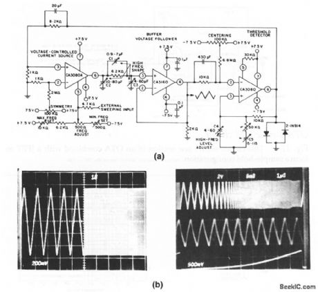
This circuit uses three sections of an OTA to form a single-control function generator that is capable of producing signals in the frequency range from 1 Hz to 1 MHz. All of the adjustments are shown on the schematic. Figure 11 -3B shows the waveforms. (View)
View full Circuit Diagram | Comments | Reading(1016)
Increasing_amplifier_output_current_and_voltage_swing
Published:2009/7/24 23:23:00 Author:Jessie
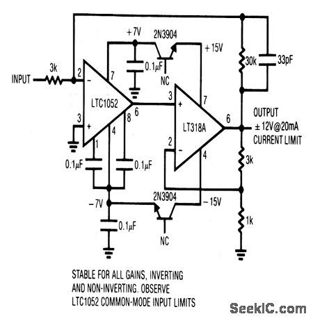
This circuit increases both the output current and the voltage-swing capability for a typical IC amplifier. The transistors run in the Zener mode, dropping the supply to about±7 V at the LTC1052. The LT318A serves as an output stage with a voltage gain of 4. The output swing is typically±13 V into 2 kΩ, with a short-circuit current of 20 mA. The circuit is dynamically stable at any gain, either inverting or noninverting. However, the LTC1052 input common-mode range (-7 V to +5 V with the ±15-V supply) must not be exceeded. (View)
View full Circuit Diagram | Comments | Reading(902)
Increasing_amplifier_output_current
Published:2009/7/24 23:22:00 Author:Jessie
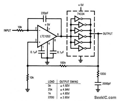
his circuit parallels a package of CMOS inverters to obtain 10- to 20-mA output current capability for a typical IC amplifier (such as an op amp). The values shown for the inversion feedback loop (10 kΩ/100 kΩ) and the RC damper (100Ω/2000 pF) are for the ICs shown. These values can be changed to accommodate other IC amplifiers. (View)
View full Circuit Diagram | Comments | Reading(820)
CLICKLESS_LEVEL_CONTROL_ATTENUATOR
Published:2009/6/29 23:47:00 Author:May
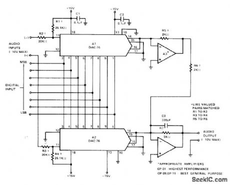
Uses two Precision Monolithics DAC-76 D/A converters to eliminate gain-change transients while providing exponential control of audio signal level. Maximum (all 1s) gain is unity from either input to output, while differential input to output gain is +6 dB. Control range is 78 dB.-W. Jung and W. Ritmanich, Audio Appli-cations for the DAC.76 Companding D/A Converter, Precision Monolithics, Santa Clara, CA, 1977, AN-28, p 4 (View)
View full Circuit Diagram | Comments | Reading(752)
_24_V_from_two_to_three_cells
Published:2009/7/24 23:21:00 Author:Jessie
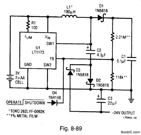
Figure 8-89 shows an LT1173 regulator connected to provide -24 V for LCD biasing using two AA cells. The 3-V input is converted to +24 V by the MOSFET switch in U1, inductor L, diode D1, and capacitor C1. The UI switch pin (SW1) then drives a charge pump composed of C2, C3, D2, and D3 to generate the -24 V.then regulation is less than 0.2% from 3.3-V to 2.0-V inputs. Load regulation, although it suffers somewhat because the -24-V output is not directly regulated, measures 2% from a 1-mA to 7-mA load. The circuit will deliver 7 mA from a 2.0-v input at 73% efficiency, and will also operate from a 5-V supply. LINEAR TECHNOLOGY, DESIGN NOTE 51, P. 1.
(View)
View full Circuit Diagram | Comments | Reading(713)
THREE_INPUT_MIXER
Published:2009/6/29 23:46:00 Author:May
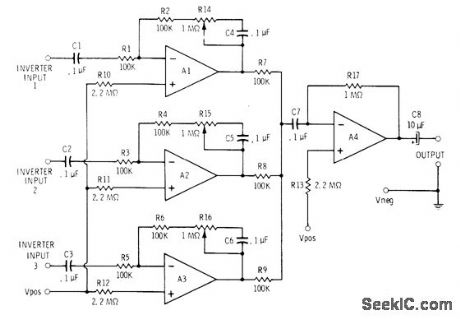
Motorola MC3401P or National LM3900 quad opamp serves for three input amplifiers each having adjustable gain range of 1 to about 11 and input impedance above about 100,000 ohms. Common outputs feed fourth opamp section connected as high-impedance amplifier. Maximum overall gain for mixeramplifier is about 300. Use well-filtered 9-15 V supply or battery capable of supplying 25 mA.-C. D. Rakes, Integrated Circuit Projects, Howard W. Sams, Indianapolis, IN, 1975, p 21-22. (View)
View full Circuit Diagram | Comments | Reading(2687)
Digitally_controlled_variable_gain_amplifier
Published:2009/7/24 23:21:00 Author:Jessie
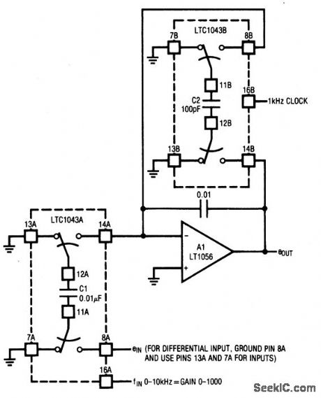
This circuit provides a continuously-variable gain from 0 to 1000, with a stability of 20 ppm/℃. Either a single-ended or differential input can be selected.A host processor selects the desired gain by applying the corresponding frequency at pin 16A of the LTC1043A. The LTC1043B is continuously clocked by a 1-kHz source (which can also be supplied by the host processor). For the values given, gain is: (fIN×10) × (0.01 μF/100 pF). Gain stability depends on the ratiometric stability between the 1-kHz clock and the variable clock (pin 16A). For this reason, both the fixed and variable clocks should be supplied by the same source (probably a processor). (View)
View full Circuit Diagram | Comments | Reading(900)
COMPRESSOR_LIM_ITER
Published:2009/6/29 23:45:00 Author:May
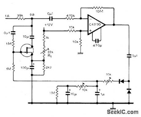
Developed for use with microphone in public-address systems.Bandwidth is 15 Hz to 25 kHz. R1 sets threshold voltage and compression law. Output of CA3130 inverting opamp is made as large as possible before being applied to rectifier and low-pass filter, to minimize effects of diode nonlinearities and capacitor leakage. Low-pass filter gives required fast attack time of about 500 ps and long decay time of about 1 min.-M. B.Taylor, Speech Compressor/Limiter, Wireless World, May 1977, p 80. (View)
View full Circuit Diagram | Comments | Reading(794)
Op_amp_full_wave_rectifier
Published:2009/7/24 21:51:00 Author:Jessie
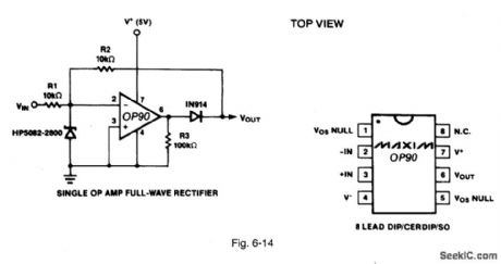
Figure 6-14 shows an OP90 connected to form a full-wave rectifier. This is similar to the circuit of Fig. 6-6, except that the OP90 has a maximum input-offset voltage of 150-μV (higher than the maximum of 70 μV for the MAX480). Similarly, the input bias current, input offset current, and drift specifications of the OP90 are higher than the MAX480. MAXIM NEW RELEASES DATA BOOK, 1993, P. 3-69. (View)
View full Circuit Diagram | Comments | Reading(1755)
SPEECH_PROCESSOR
Published:2009/6/29 23:44:00 Author:May
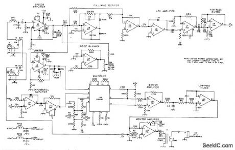
Can improve signal strength and intelligibility of voice signals up to 6 dB without unpleasant changes in fidelity.Used between microphone and input of AM or SSB transmitter. Based on separation of signal envelope from constant-amplitude carrier that together make up voice signal. After Iogamp U6 separates components of speech waveform, envelope is filtered out by cative RC high-pass filter U8 having 50.Hz cutoff, with exactly unity gain above cutoff. Filtered signal goes to ex-ponential amplifier U9-U10 and is then multi-plied by correct sign information in U14. Sign information is obtained by hard-Iimiting input voice signal with diode clipper CRS-CR6. Re-sulting square-wave output is multiplied by sig-nal from UJT in U14. Processed signal goes to transmitter input through low-pass filter U12 having sharp cutoff above 3 kHz to eliminate unwanted high-frequency energy. CR1-CR4 are 1N914 or other matched silicon diodes. T1 is 250-mW audio transformer. Article gives con-struction and adjustment details.-J. E. Kauf-mann and G. E. Kopec, A Homomorphic Speech Compressor, QST, March 1976, p 33-37. (View)
View full Circuit Diagram | Comments | Reading(0)
Low_noise_microphone_preamplifier
Published:2009/7/24 21:50:00 Author:Jessie

Figure 6-13 shows an OP27 connected as a low-noise microphone preamp. The input voltage noise is 3 nV√Hz at 1 kHz. The OP27 has an 8-MHz gain-bandwidth product and a 2.8-V/μs slew rate. The OP37 has a 63-MHz gain-bandwidth with a 17-V/μs slew rate. Input-offset voltage is 10 μV, drift is 0.2 μV/℃, and output swing is ±10 V into 600 Ω. MAXIM NEW RELEASES DATA BOOK, 1993, P. 3-67. (View)
View full Circuit Diagram | Comments | Reading(169)
EXPANDER
Published:2009/6/29 23:40:00 Author:May
Uses Signetics dual-channel compandor IC; 571 has lower inherent distortion and higher supply voltage range (6-24 V) than 571 (6-18 V). Values shown are for 15-V supply with either IC. Gain through expander is 1.43 VIN, where VIN is average input voltage. Unity gain occurs at RMS input level of 0.775V, or 0 dBm in 600-ohm systems.-W.G.Jung, Gain Control IC for Audio Signal Processing, Ham Radio, July 1977, p 47-53. (View)
View full Circuit Diagram | Comments | Reading(2018)
| Pages:1235/2234 At 2012211222122312241225122612271228122912301231123212331234123512361237123812391240Under 20 |
Circuit Categories
power supply circuit
Amplifier Circuit
Basic Circuit
LED and Light Circuit
Sensor Circuit
Signal Processing
Electrical Equipment Circuit
Control Circuit
Remote Control Circuit
A/D-D/A Converter Circuit
Audio Circuit
Measuring and Test Circuit
Communication Circuit
Computer-Related Circuit
555 Circuit
Automotive Circuit
Repairing Circuit