
Circuit Diagram
Index 1231
DELAYED_ALARM
Published:2009/6/30 1:45:00 Author:May
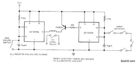
When normally closed arm/disarm switch is opened, first section of NE556 dual timer starts its timing cyde. After delay to allow for entry or exit, pin 5 goes low to energize alarm circuit. Now as long as all door switches are dosed, PNP transistor is kept off because pin 9 is high. When any door switch is opened, transistor tums on after normal delay for owner to enter car, and hom is sounded unless owner closes arm/disarm switch within delay time.- Signetics Analog Data Manual, Signetics, Sunnyvale, CA, 1977, p 724-725. (View)
View full Circuit Diagram | Comments | Reading(0)
SILENT_ALARM
Published:2009/6/30 1:44:00 Author:May
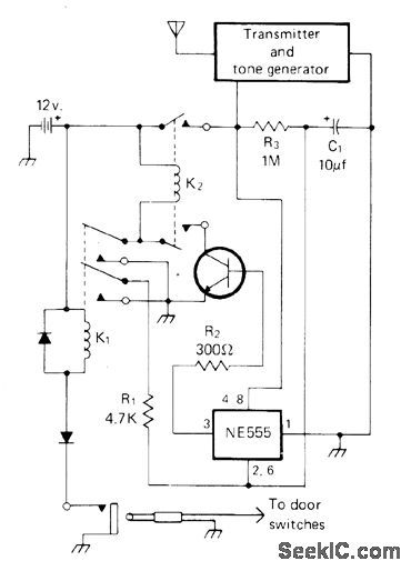
When thief opens car door, relays K1 and K2 activate tone-modulated transmitter, which can be any legal combination of power, frequency, and antenna. A few milliwatts of power should be adequate. Thief hears nothing, but owner is alerted via portable receiver tuned to transmitter frequency. Transmitter remains on about 15 s (determined by R3 and C1) after door is closed until NE555 times out and removes power from transistor. Use any NPN transistor having adequatecurrent rating for relay. If alarm is provided with its own battery and whip antenna, it cannot be disabled from outside of car.-A. Day, Soundless Mobile Alarm, CQ, April 1977, p 11. (View)
View full Circuit Diagram | Comments | Reading(0)
VOICE_DIGITIZER
Published:2009/6/30 1:44:00 Author:May
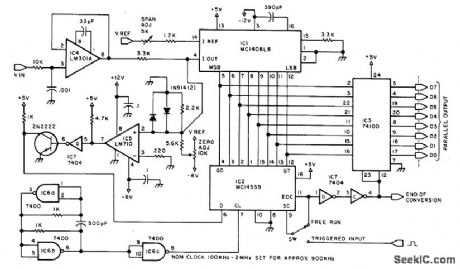
Uses 8-bit ADC capable of sampling AF input signal 100,000 times per second when using 900-kHz clock. 100-kHz clock gives 9000 samples per second, about minimum for human voice. Digital output is stored in computer memory for later conversion back to analog form for such applications as synthesis of speech from phonemes and providing voice answers to queries. Requires about 10,000 bytes in memory for 1 s of voice data. Pin 7 of IC4 is +12 V, and pin 4 is -6 V. For IC6 and IC7, pin 14 is +5 V and pin 7 is ground. 8080 assembler programs are given for input and output of memory.—S. Ciarcia, Talk to Me! Add a Voice to Your Computerfor $35, BYTE, June 1978, p 142-151. (View)
View full Circuit Diagram | Comments | Reading(1802)
MOSFET_INPUT_BUFFER
Published:2009/6/30 1:42:00 Author:May


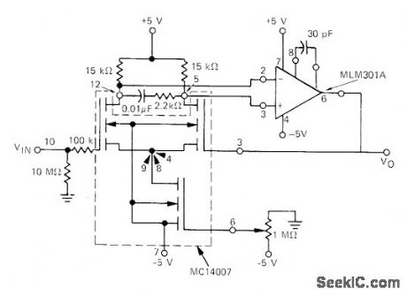
Uses Motorola MC14007 dual complementary pair plus inverter, with two of MOSFETs connected as differential amplifier for buffering opamp and third serving as current source for differential amplifier. Arrangement gives high input impedance required in some applications of MC1505 A/D converter for which buffer was designed. 1-megohm pot controls gate voltage for current source. Temperature drift is well under 2 mV over range of 0-50℃. Pin 14 of MC14007 should be tied to +5 V.—D. Aldridge and S. Kelley, Input Buffer Circuits for the MC1505 Dual Ramp A-to-D Converter Subsystem, Motorola, Phoenix, AZ, 1976, EB-24A. (View)
View full Circuit Diagram | Comments | Reading(2046)
CAR_THEFT_ALARM
Published:2009/6/30 1:42:00 Author:May
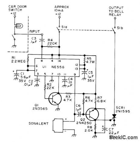
Alarm remains on even if signal from car door switch or other sensor is only momentary, so relay is wired to be selflatching until keyswitch S1 is tumed off. Use hood locks or hood-opening sensors to prevent thief from disabling alarm by cutting battery cable. Circuit indudes time delay of 6 s for entering car and shutting off alarm, to avoid need for extemal keyswitch. Sonalert makes loud tone during 6-s delay period to remind driver that alarm needs to be turned off. At end of 6 s, Sonalert stops and much louder bell is energized to further discourage intruder.-J. Pawlan, The Smart Alarm, 73 Magazind, June 1975. p 37-41. (View)
View full Circuit Diagram | Comments | Reading(1021)
EXTERNAL_TRlGGER
Published:2009/6/30 1:41:00 Author:May
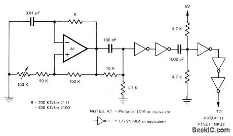
Generates pulse with 100-ns minimum width in range of 125-250 Hz for application to reset input of Teledyne Philbrick A/D converter in applications requiring un attended operation with continuous conversion. Adjust 100K pot to give 125 Hz for 4109 or 250 Hz for 4111. Successive stages of SN7404 inverter provide required sharpening of pulse.A1 is positive-starting MVBR.—R. W. Jacobs, Repetitive Mode Operation for Models 4109/4111 Integrating A/D Converters, Teledyne Philbrick, Dedham, MA, 1977, AN-28. (View)
View full Circuit Diagram | Comments | Reading(933)
CASCODE_TONE_CONTROL
Published:2009/6/30 1:41:00 Author:May
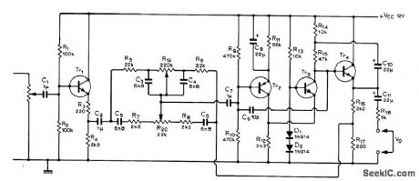
Circuit raises 100-mV input signal level to 1V for driving power amplifier and uses cascode arrangement to im-prove S/N ratio of tone control network. Values show give maximum bass boost or cut at 50Hz with R19 and maximum treble boost or cut at 10kHz with R20,Tr2 can be BC15,BC214、BC309, or equivalent,Other transistors can be BC109、BC114、BC184, or equivalent.-J,N Ellis,Hiah Quality Tone Control, Wireless World Aug.1973、p378 (View)
View full Circuit Diagram | Comments | Reading(2245)
14_V_MAXIMUM
Published:2009/6/29 22:04:00 Author:May
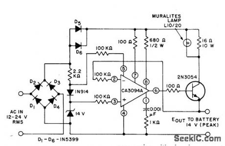
Circuit accurately limits peak output voltage to 14 V, as established by zener connected between terminals 3 and 4 of CA3094A programmable opamp. Lamp brightness varies with charging current. Reference voltage supply does not drain battery when power supply is disconnected.- Circuit Ideas for RCA Linear ICs, RCA Solid State Division, Somerville, NJ, 1977, p 19. (View)
View full Circuit Diagram | Comments | Reading(813)
Fiber_optic_receiver
Published:2009/7/24 21:03:00 Author:Jessie
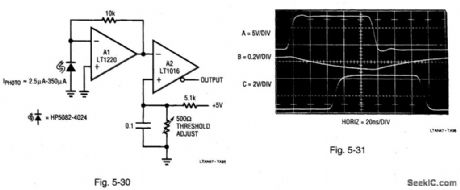
Figure 5-30 shows a simple, high-speed fiber-optic receiver. Figure 5-31 shows the waveforms. Trace A is a pulse associated with a photo input. Trace B is the A1 response, and trace C is the A2 output. A2 compares the A1 output to a dc level that is established by the threshold-adjust setting, thus producing a logic-compatible output. LINEAR TECHNOLOGY, APPLICATION Nom 47, P. 43. (View)
View full Circuit Diagram | Comments | Reading(2502)
Fast_photo_integrator
Published:2009/7/24 21:02:00 Author:Jessie
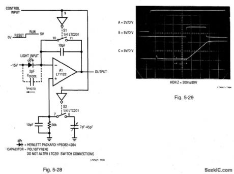
Figure 5-28 shows a photodiode-amplifier circuit that was specifically designed for situations where the total energy In a light pulse(or pulses)must be measured,The circuit is a very fast integrator, with S1 used as a reset switch, S2,switched simultaneously with S1, compensated the 51 charge-injection error. With the control input(trace A, Fig.5-29)low,and no photocurrent,51 is closed and A1 looks like a grounded follower. Under these conditions, the A1 output(trace C) remains 0 V. When the control input becomes high,A1 becomes an integrator as soon as S1 opens. At this point, the integrator is ready to receive and record a photo pulse. When light falls on the photodiode (trace B triggers a light pulse seen by the photodiode), A1 responds by integrating, and the A1 voltage (after the light event is over) is related to the total energy at the diode during the event. To adjust, cover the photodiode and set the trimmer capacitor for 0-V output from A1 (immediately after the S1/S2 switching function). LINEAR TECHNOLOGY, APPLICATION NOTE 47, P. 42. (View)
View full Circuit Diagram | Comments | Reading(2061)
Photodiode_amplifier
Published:2009/7/24 21:00:00 Author:Jessie
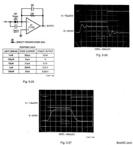
Figure 5-25 shows a basic photodiode amplifier. The table shows various circuit outputs for different diode currents. Figure 5-26 shows circuit response to a photo input (trace A) with the 3-pF feedback capacitor removed. Notice that the output overshoots and saturates before finally ringing down to a level value. Figure 5-27 shows circuit performance with the 3-pF feedback capacitor in place. The same input pulse (trace A, Fig. 5-27) produces a cleanly damped output (trace B).However, the circuit is about 50% faster with the feedback capacitor removed. LINEAR TECHNOLOGY, APPLICATION NOTE 47, P. 41, 42. (View)
View full Circuit Diagram | Comments | Reading(0)
Differential_comparator_amplifier_with_adjustable_limiting_and_offset
Published:2009/7/24 20:59:00 Author:Jessie
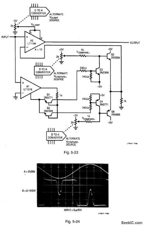
Figure 5-23 is similar to Fig. 5-21, except that the dual channels permit observations of information between two adjustable amplitude-defined points. The set points are adjustable in both magnitude and sign. In the circuit of Fig. 5-23, the polarity of the offset applied to the A2 inverting input is determined by the comparator A1 output state. Figure 5-24 shows the circuit output for a sine input (trace A). The +VCOMPARE and -VCOMPARE voltages are set just below the sine-wave peaks, with VCLAMP set to restrict amplification to the peak excursion. The circuit output (trace B) simultaneously shows the amplitude detail of both sine peaks. LINEAR TECHNOLOGY, APPLICATION NOTE 47, P. 40, 41. (View)
View full Circuit Diagram | Comments | Reading(733)
Notebook_computer_porter_management
Published:2009/7/24 20:59:00 Author:Jessie
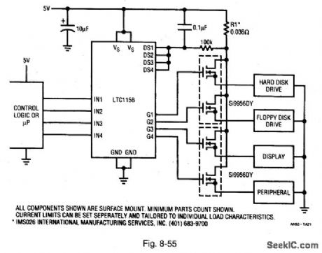
Figure 8-55 shows an LTC1156 connected to control power (and protect) for components of a notebook computer (or similar device). Each load in the circuit is activated by the microprocessor only when that component is required to process or display information. When not needed (as determined by microprocessor control), the individual systems are placed in the standby mode where quiescent current is reduced to microamp levels. The standby current of the LTC1156 is typically 16 μA with all four inputs turned off. LINEAR TECHNOLOGY, APPLICATION NorE 53, P. 10. (View)
View full Circuit Diagram | Comments | Reading(678)
Fast_differential_comparator_amplifier_with_adjustable_offset
Published:2009/7/24 20:57:00 Author:Jessie

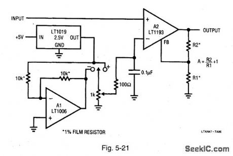
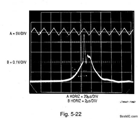
Figure 5-21 shows a circuit that permits one particular portion of a signal to be amplified (or examined) with all other portions rejected. Figure 5-22 shows what happens when the output of a triangle-wave generator (trace A) is applied to the circuit. Setting the bias level just below the triangle peak permits high-gain, detailed observation of the turnaround at the peak. Switching residue in the generator output is observable in trace B. Appropriate variations in voltage-source setting will permit more of the triangle slopes to be observed, (with a loss of resolution because of scope-overload). Similarly, increasing the A2 gain allows more amplitude detail, while placing restrictions on how much of the waveform can be displayed. In effect, this circuit performs the same functions as differential plug-in units for scopes. The circuit output is accurate and settled to 0.1% about 100 ns after entering the linear region. LINEAR TECHNOLOGY, APPLICATION NOTE 47, P. 39, 40. (View)
View full Circuit Diagram | Comments | Reading(760)
Suzuki elevator brake circuit (B)
Published:2011/7/23 10:41:00 Author:John | Keyword: elevator brake
View full Circuit Diagram | Comments | Reading(758)
Switch_driver_with_micropower_standby_mode_18_V_to_28_V
Published:2009/7/24 20:56:00 Author:Jessie

Figure 8-54 shows an LTC1155 connected for switchldriver operation with micropower standby. This circuit is similar to that shown in Fig. 8-53, but with R1 increased from 3 kΩ to 330 kΩ, and a boot-strap R2/D2 network added. These modifications reduce the Fig. 8-54 standby current to less than 30 μA. The extra supply current is provided only when the switch is turned on. The supply current drops back to 30 μA when the switch is turned off, and the LTC1155 is returned to standby. LINEAR TECHNOLOGY, APPLICATION NOTE 53, P. 4, (View)
View full Circuit Diagram | Comments | Reading(608)
Transistor regulator
Published:2011/7/23 10:39:00 Author:John | Keyword: Transistor regulator
View full Circuit Diagram | Comments | Reading(856)
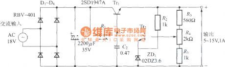
Solar Garden Light
Published:2011/7/23 10:37:00 Author:John | Keyword: Solar Garden Light
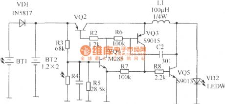
Solar garden light is as shown. When there is sunlight in the day, light energy is transferred into electrical energy by BT1. And BT2 charges the VD1. Due to the light, photosensitive resistor is with low resistance. VQ4 b closes due to very low electrical level. When there is no light at night, the photosensitive resistor is with high resistance. So VQ4 conducts. VQ2b also conducts due to very low electrical level. When the DC boost circuit composed of VQ3, VQ5, C2, R6 and L1 starts to work, LED powers to get light. The core of the DC boost circuit is a complementary tube oscillator circuit. (View)
View full Circuit Diagram | Comments | Reading(2038)
Transformer_coupled_amplifier
Published:2009/7/24 20:56:00 Author:Jessie
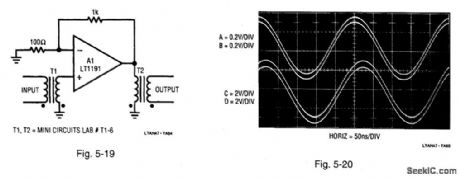
Figure 5-19 shows another way to get high common-mode rejection, together with true 3-port isolation. The input, gain stage, and output are all galvanically isolated from each other. As such, this circuit is useful where large common-mode differences are encountered or where ground integrity is uncertain. With the values shown, A1 has a gain of 11. T1 feeds the A1 input, and the output is taken from T2.Figure 5-20 shows results for a 4-MHz input, with all of the polarity dots referred to ground. The input (trace A, Fig. 5-20) is applied to T1. The output of T1 (trace B) feeds A1. A1 produces gain, and the A1 output (trace C) feeds T2. The T2 output (trace D) is the circuit output. Using the specified transformers, the low-frequency cutoff is about 10 kHz. LINEAR TECHNOLOGY, APPLICATION (View)
View full Circuit Diagram | Comments | Reading(913)
High_speed_differential_line_receiver
Published:2009/7/24 20:55:00 Author:Jessie
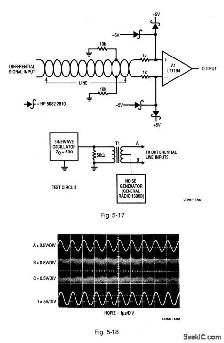
Figure 5-17 shows a simple, fast differential line receiver using an LT1194 gain-of-ten amplifier. A test circuit is also included on Fig. 5-17. Figure 5-18 shows the test results. The sine-wave oscillator drives T1 (trace A, Fig. 5-18), producing a differential-line output at the secondary. The T1 secondary is returned to ground through a broadband noise generator, flooding the inputs with common-mode noise (traces B and C are A1 inputs.) Trace D, the A1 ×10 version of the differential signal at the input, is clean with no visible noise or disturbances, in spite of the 100:1 noise-to-signal radio. LINEAR TECHNOLOGY, APPLICATIONS NOTE 47, P. 38. (View)
View full Circuit Diagram | Comments | Reading(830)
| Pages:1231/2234 At 2012211222122312241225122612271228122912301231123212331234123512361237123812391240Under 20 |
Circuit Categories
power supply circuit
Amplifier Circuit
Basic Circuit
LED and Light Circuit
Sensor Circuit
Signal Processing
Electrical Equipment Circuit
Control Circuit
Remote Control Circuit
A/D-D/A Converter Circuit
Audio Circuit
Measuring and Test Circuit
Communication Circuit
Computer-Related Circuit
555 Circuit
Automotive Circuit
Repairing Circuit