
Circuit Diagram
Index 1229
WINDOW_FOIL_ALARM
Published:2009/6/30 2:03:00 Author:May
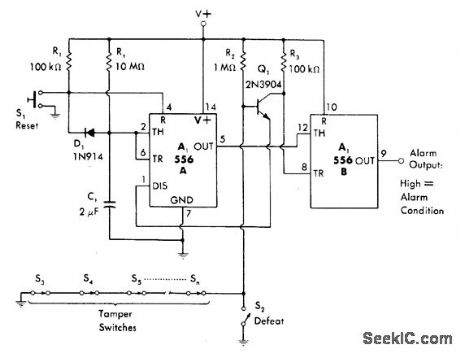
Combination of power-up mono MVBR and latch, using both sections of 556 timer, drives output line high when sensor circuit is opened at door or window switch or by breaking foil on glass. Once alarm is triggered, reclosing of sensor has no effect; S1 must be closed momentarily after restoring sensor circuit to tum alarm off. Circuit includes 22-s power-up delay that prevents triggering of alarm when it is first turned on.-W. G. Jung, IC Timer Cookbook, Howard W. Sams, Indianapolis, IN, 1977, p 231-232. (View)
View full Circuit Diagram | Comments | Reading(1888)
01_Hz_TO_10_Hz_BANDPASS_FILTER
Published:2009/6/30 2:03:00 Author:May
View full Circuit Diagram | Comments | Reading(989)
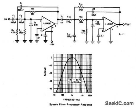
SPEECH_FILTER(300_Hz3_kHz_BANDPASS)
Published:2009/6/30 2:02:00 Author:May
View full Circuit Diagram | Comments | Reading(1156)
2_V_TO_2O_AND_15O_V
Published:2009/6/30 2:02:00 Author:May
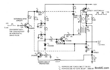
Use of 7-turn toroidal transformer in self-excited dnging-choke blocking-oscillator circuit improves efficiency of converter circuit by providing fast switching time. Circuit is practical only when input and output voltages differ signfficantly. Blocking oscillator is formed by Q1, T2, C1, R2, and base-bias network R6-Q2. Q4 makes possible external synchronization, permitting use in television systems for triggering regulator with leading edge of horizontal drive pulse. This ensures completion of cycle within blanking interval.—N. Tkacenko, Transformer Increases DC-DC Converter Efficiency to 80%, EDN Magazine, May 5, 1976, p 110 and 112. (View)
View full Circuit Diagram | Comments | Reading(1379)
1_12_V_TO__12_V
Published:2009/6/30 2:00:00 Author:May
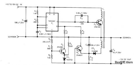
Transforms unregulated +12 VDC to current-Iimited regulated -12 VDC. Front end of 555 is connected in astable configuration, with R2 selected to give about 25 kHz at pin 3. Control of modulation input to pin 5 gives voltage regulation and current limiting. Circuit tolerates continuous operation under short-circuit conditions. With 10-V nominal output, line regulation is within 0.05% for input and output voltage ranges of 0.3 to 10 V. Load regulation is 0.2% for loads from 10 μA to 10mA when load impedance is 10 ohms,—R.Dow,Build a Short-Circuit-Proof +12V Inverter,with One IC,EDN Magazine,Sept 5,1977,p 177-178 (View)
View full Circuit Diagram | Comments | Reading(985)
Wien_bridge_oscillator_with_common_mode_suppression
Published:2009/7/24 20:36:00 Author:Jessie
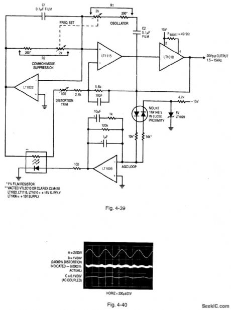
Figure 4-39 shows another version of the Fig. 4-34 circuit, but with automatic trim and common-mode suppression (similar to that of Fig. 4-28). The circuit output (trace A, Fig. 4-40) contains less than 0.0003% (3 ppm) distortion (trace B), with no visible correlation to gain-loop ripple residue (trace C). This level of distortion is below the uncertainty floor of most distortion analyzers. LINEAR TECHNOLOGY, APPLICATION NOTE 43, P. 32, 33. (View)
View full Circuit Diagram | Comments | Reading(693)
POLE_ACTIVE_LOW_PASS_FILTER(B_UTTERWORTH_MAXIMALLY_FLAT_RESPONSE)
Published:2009/6/30 2:00:00 Author:May
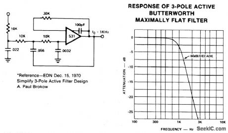
View full Circuit Diagram | Comments | Reading(799)
Feedback_measurement
Published:2009/7/24 20:36:00 Author:Jessie
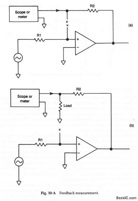
Because op-amp circuits usually include feedback, it is sometimes necessary to measure feedback voltage at a given frequency with given operating conditions.The basic feedback-measurement connections are shown in Fig. 10-A. Although it is possible to measure the feedback voltage, as shown in Fig. 10-Aa, a more accurate measurement is made when the feedback lead is terminated in the normal operating impedance(Fig.10-Ba).If an input resistance is used In thecircuit,and this resistance is considerably lower than the IC inputimpedance,usethe resistance value.If In doubt, measure the input impedance of the IC(asdescribed In chapter 1). Then,terminate the feedback lead In that value(tomeasure open-loop feedback voltage). Remember that open-loop voltage gammust be substantially higher than the closed-loop voltage gam for most Op-ampcircuits to perform properly. (View)
View full Circuit Diagram | Comments | Reading(689)
_12_V_TO__12_V
Published:2009/6/30 1:59:00 Author:May
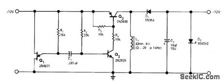
Transformerless inverting DC-to-DC converter has above 55% effciency and can withstand output shorts lasting up to several minutes. UJT Q1 and base-emitter diode of transistor Q2 from free-running MVBR whose 25-kHz output is amplified by Q2 to drive switching-mode converter Q3-L1-D1-C2. Zener D2 regulates output for variations in input voltage or output loads up to 40 mA.—G. Bank, Transformerless Converter Supplies Inverted Output, EDN|EEE Magazine, July 1, 1971, p 48. (View)
View full Circuit Diagram | Comments | Reading(1060)
4_BIT_CLOCKLESS
Published:2009/6/30 1:56:00 Author:May

Simple and low-cost arrangement of seven CA3130 opamps gives conversion times fast enough for tracking sinewave signals well up into audio range, Even with relatively slow 741 opamps, signals up to 300 Hz were easily tracked. Additional bits are easily cascaded.—B. P. Vandenberg, Tracking-Type A/D Requires No Clock Oscillator, EDN Magazine, Jan. 20, 1977, p 92 and 94. (View)
View full Circuit Diagram | Comments | Reading(1173)
Wien_bridge_oscillator_with_automatic_trim
Published:2009/7/24 20:35:00 Author:Jessie
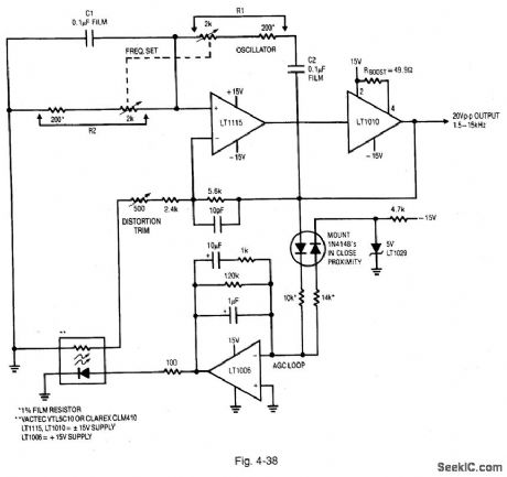
Figure 4-38 shows another version of the Fig. 4-34 circuit, but with automatic trim for distortion. Q1 is replaced with an optically driven CdS photocell, and the LT1055 is replaced with a ground-sensing op amp operating in the single-supply mode. Distortion improves slightly to 0.0015%. LINEAR TECHNQLOGY, APPLICATION NOTE 43, P. 33. (View)
View full Circuit Diagram | Comments | Reading(820)
Wien_bridge_oscillator_with_improved_stabilization
Published:2009/7/24 20:33:00 Author:Jessie
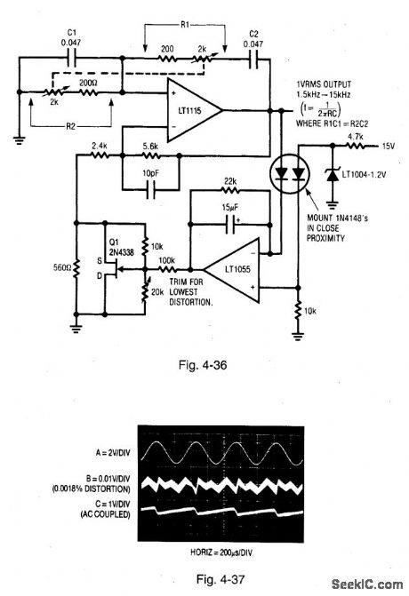
Figure 4-36 shows an improved version of the Fig. 4-34 circuit. Figure 4-37 shows waveforms for the Fig. 4-36 circuit. The 20-kΩ trimmer in the Q1 circuit makes it possible to get 0.0018% distortion (trace B, Fig. 4-37). LINEAR TECHNOLOGY, APPLICATION NOTE 43, P. 31. (View)
View full Circuit Diagram | Comments | Reading(697)
FILTERED_BUFFER
Published:2009/6/30 1:55:00 Author:May
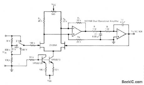
Used with Motorola MC1505 AiD converter when making precise measurements of slowly varying DC voltages in digital voltmeters or in feedback controls.Closed-loop front-end buffer provides high input impedance and reduces stray noise and 60-Hz pickup. Two-pole filter is included in unity-feedback loop of buffer. Front-end scaling circuit is induded with buffer.—D. Aldridge and S. Kelley, Input Buffer Circuits for the MC1505 Dual Ramp A-to-D Converter Subsystem, Motorola, Phoenix, AZ, 1976, EB-24A. (View)
View full Circuit Diagram | Comments | Reading(1038)
MULTIPLEXED_BURGLAR_ALARM
Published:2009/6/30 1:54:00 Author:May
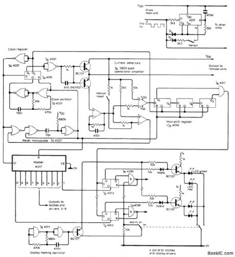
Multiplexing technique provides for detection of state of up to 10 sensors, with immediate identification and location of activated sensor. Only one pair of wires runs from control unit to paralleled remote sensor circuits, one of which is shown at upper right. Each sensor location uses different output from one to zero. Multiplexor circuit is based on 4017 decade counter having 10 individual outputs, to give signals in 10 time slots. Power supply rail is used to reset counter. Clock line is eliminated by switching supply line as square wave. Sensor indication line is eliminated by detecting power supply current drain. Control unit uses oscillator and shift register to generate clocking waveforms. 3900 quad opamp converts sensorline current to logic levels for clocking by master 4017 to control 10 out-put latches and display driver. Two consecutive sensor-open signals are required to activate alarm, minimizing false alarms by interference pulses.-R. J. Chance, Multiplexed Alarm, Wireless World, Nov 1978, p 73-74. (View)
View full Circuit Diagram | Comments | Reading(1638)
Wien_bridge_sine_wave_oscillator_with_electronic_amplitude_stabilization
Published:2009/7/24 20:31:00 Author:Jessie
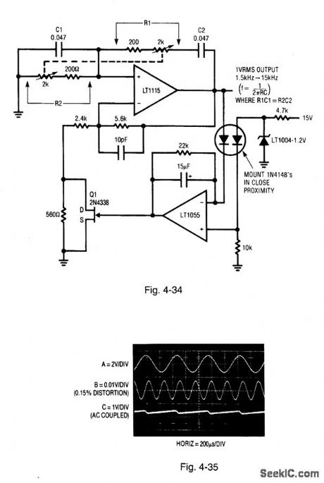
Figure 4-34 shows a sine-wave oscillator that uses electronic stabilization in place of the lamp. Figure 4-35 shows the waveforms. Trace A shows the output. Trace B shows distortion, and trace C shows the rectifier peaking residue at the Q1 gate. LINEAR TECHNOLOGY, APPLICATION NOTE 43, P. 30, 31. (View)
View full Circuit Diagram | Comments | Reading(735)
8_BIT_DIGlTAL_OUTPUT
Published:2009/6/30 1:54:00 Author:May
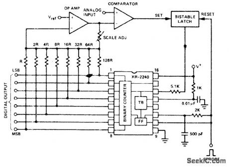
Digital output is obtained in parallel format from binary-counter output of Exar XR-2240 programmable timer/counter. Recycle time is about 6 ms. Supply voltage can be 4-15 V.— Timer Data Book, Exar Integrated Systems, Sunnyvale, CA, 1978, p 11-18. (View)
View full Circuit Diagram | Comments | Reading(1546)
HI_FI_EXPANDER
Published:2009/6/30 1:54:00 Author:May
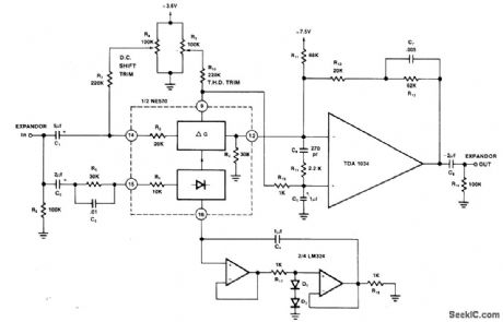
Used in playback of material that has been recorded with overload-prevent ing compressor. Extemal opamp is used for high slew rate. Adjust distortion trimpot Rg for minimum total harmonic distortion-when using input of 0 dBm at 10 kHz. Adjust DC shift pot Re after this, for minimum envelope bounce with tone-burst input,-″Signetics Analog Data Manual,″ Signetics, Sunnyvale,CA,1977,p 804-805. (View)
View full Circuit Diagram | Comments | Reading(1034)
REMOTE_STATION
Published:2009/6/30 1:54:00 Author:May
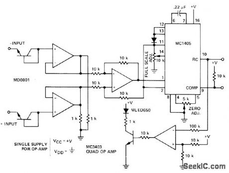
Multiplexing of large number of analog voltages from widely separated locations in large industrial control systems is simplified by transmitting two noise-immune low-frequency digital signals from each remote to central multiplexet driving display and microprocessor. Central station using MC14435 controls direction of integration in each remotestation MC1405 through ramp control output.At beginning of conversion, integrator of MC1405 integrates upward for 1000 counts of central-station clock. Integrator then ramps down while comparator remains high, with clock continuing until comparator threshold is again crossed. Counts during down ramp are latched by counter when comparator goes low, and circuits are reset for next conversion. Analog input voltage is thus transmitted to central-station MC14435 astwo digital signals.—S. Kelley, Analog Data Acquisition Network for Digital Processing Using the MC1405-MC14435 A/D System, Motorola, Phoenix, AZ, 1975, EB-58. (View)
View full Circuit Diagram | Comments | Reading(1258)
Multi_range_Wien_bridge_sine_wave_oscillator
Published:2009/7/24 20:29:00 Author:Jessie
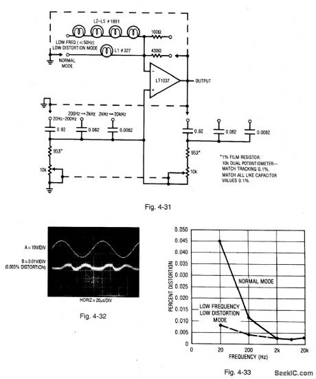
Figure 4-31 shows a Wien-bridge sine-wave oscillator with a frequency range from 20 Hz to 20 kHz, in three decade ranges, with 0.25-dB amplitude flatness. Trace A of Fig. 4-32 shows circuit output at 10 kHz. Trace B shows distortion (below 0.003%). Figure 4-33 plots distortion versus frequency. LINEAR TECHNOLOGY, APPLICATION NOTE 43, P. 29, 30. (View)
View full Circuit Diagram | Comments | Reading(815)
BAXANDALL_TONE_CONTROL
Published:2009/6/30 1:53:00 Author:May
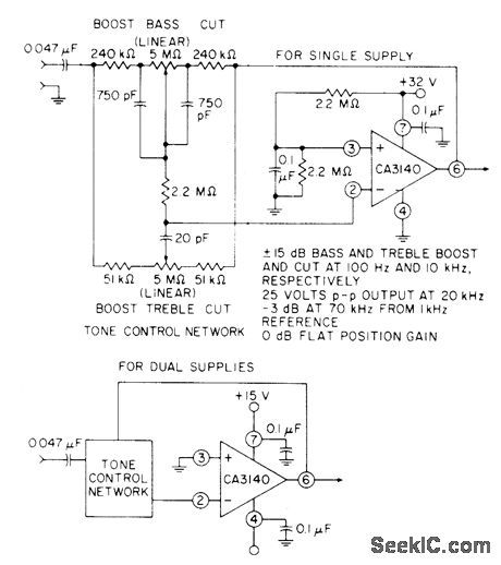
Utilizes high slew rate, high output-voltage capability, and high input impedance of CA3140 bipolar MOS opamp to provide unity gain at midband along with bass and treble boost and cut of ±15dB at 100 and 10,000 Hz. Optional connection for ±15 V supply is shown below.- Circuit Ideas for RCA Linear ICs, RCA Solid State Division, So-merville, NJ, 1977, p 10. (View)
View full Circuit Diagram | Comments | Reading(2166)
| Pages:1229/2234 At 2012211222122312241225122612271228122912301231123212331234123512361237123812391240Under 20 |
Circuit Categories
power supply circuit
Amplifier Circuit
Basic Circuit
LED and Light Circuit
Sensor Circuit
Signal Processing
Electrical Equipment Circuit
Control Circuit
Remote Control Circuit
A/D-D/A Converter Circuit
Audio Circuit
Measuring and Test Circuit
Communication Circuit
Computer-Related Circuit
555 Circuit
Automotive Circuit
Repairing Circuit